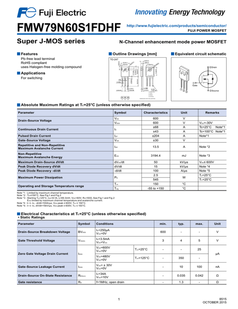
FMW79N60S1FDHF
Super J-MOS series
http://www.fujielectric.com/products/semiconductor/
FUJI POWER MOSFET
N-Channel enhancement mode power MOSFET
Features
Outline Drawings [mm]
Pb-free lead terminal
RoHS compliant
uses Halogen-free molding compound
Equivalent circuit schematic
TO-247
②Drain
Applications
For switching
①
②
①
Gate
③
①
②
③
③Source
Characteristics
Unit
Remarks
V
V
A
A
A
V
VGS =-30V
Tc=25°C Note*1
Tc=100°C Note*1
Note*1
CONNECTION
① GATE
② DRAIN
③ SOURCE
①
②
③
DIMENSIONS ARE IN MILLIMETERS.
Absolute Maximum Ratings at TC =25°C (unless otherwise specified)
Parameter
Symbol
Drain-Source Voltage
VDS
VDSX
Continuous Drain Current
ID
Pulsed Drain Current
Gate-Source Voltage
IDP
VGS
600
600
±68
±43
±204
±30
Repetitive and Non-Repetitive
Maximum Avalanche Current
IAR
13.5
A
Note *2
Non-Repetitive
Maximum Avalanche Energy
EAS
3194.4
mJ
Note *3
Maximum Drain-Source dV/dt
Peak Diode Recovery dV/dt
Peak Diode Recovery -di/dt
dVDS /dt
dV/dt
-di/dt
kV/μs
kV/μs
A/μs
Maximum Power Dissipation
PD
Operating and Storage Temperature range
Tch
Tstg
50
15
100
2.5
545
150
-55 to +150
W
VDS ≤ 600V
Note *4
Note *5
Ta=25°C
TC =25°C
°C
°C
Note *1 : Limited by maximum channel temperature.
Note *2 : Tch ≤150°C, See Fig.1 and Fig.2
Note *3 : Starting Tch =25°C, IAS=8.1A, L=89.3mH, VDD =60V, RG =50Ω, See Fig.1 and Fig.2
E AS limited by maximum channel temperature and avalanche current.
Note *4 : I F ≤ -I D, -di/dt=100A/μs, VDS peak ≤ 600V, Tch ≤ 150°C.
Note *5 : I F ≤ -I D, dV/dt=15kV/μs, VDS peak ≤ 600V, Tch ≤ 150°C.
Electrical Characteristics at TC =25°C (unless otherwise specified)
• Static Ratings
Parameter
Symbol
Conditions
min.
typ.
max.
Unit
Drain-Source Breakdown Voltage
BVDSS
ID =250μA
VGS =0V
600
-
-
V
Gate Threshold Voltage
VGS(th)
ID =3.5mA
VDS =VGS
3
4
5
V
Zero Gate Voltage Drain Current
IDSS
VDS =600V
VGS =0V
Tch=25°C
-
-
25
VDS =480V
VGS =0V
Tch=125°C
-
350
-
μA
Gate-Source Leakage Current
IGSS
VGS = ± 30V
VDS =0V
-
10
100
nA
Drain-Source On-State Resistance
RDS(on)
ID =34A
VGS =10V
-
0.035
0.042
Ω
Gate resistance
RG
f=1MHz, open drain
-
1.3
-
Ω
1
8515
OCTOBER 2015
FMW79N60S1FDHF
FUJI POWER MOSFET
http://www.fujielectric.com/products/semiconductor/
• Dynamic Ratings
Parameter
Symbol
Conditions
min.
typ.
max.
Unit
Forward
Transconductance
gfs
ID =34A
VDS =25V
26
53
-
S
Input Capacitance
Output Capacitance
Reverse Transfer Capacitance
Ciss
Coss
Crss
VDS =400V
VGS =0V
f=250kHz
-
5970
180
12
-
Effective output capacitance,
energy related (Note *6)
Co(er)
VGS =0V
VDS =0…400V
-
450
-
Effective output capacitance,
time related (Note *7)
Co(tr)
VGS =0V
VDS =0…400V
ID =constant
-
1585
-
-
186
32
205
20
209
53
93
27
-
Turn-On Time
Turn-Off Time
Total Gate Charge
Gate-Source Charge
Gate-Drain Charge
Drain-Source crossover Charge
td(on)
tr
td(off)
tf
QG
QGS
QGD
QSW
VDD =400V, VGS =10V
ID =34A, RG =8.2Ω
See Fig.3 and Fig.4
VDD =400V, ID =68A
VGS =10V
See Fig.5
pF
ns
nC
Note *6 : C o(er) is a fixed capacitance that gives the same stored energy as C oss while VDS is rising from 0 to 400V.
Note *7 : C o(tr) is a fixed capacitance that gives the same charging times as C oss while VDS is rising from 0 to 400V.
• Reverse Diode
Parameter
Symbol
Conditions
min.
typ.
max.
Unit
Avalanche Capability
IAV
L=19.3mH, Tch=25°C
See Fig.1 and Fig.2
13.5
-
-
A
Diode Forward On-Voltage
VSD
IF=68A, VGS =0V
Tch=25°C
-
1.1
1.35
V
Reverse Recovery Time
trr
230
-
ns
Reverse Recovery Charge
Qrr
-
1.9
-
μC
Peak Reverse Recovery Current
Irp
-
16
-
A
min.
typ.
max.
Unit
-
-
0.23
50
°C/W
°C/W
IF=68A, VDD =400V
-di/dt=100A/μs
Tch=25°C
See Fig.6 and Fig.7
Thermal Resistance
Parameter
Symbol
Channel to Case
Channel to Ambient
Rth(ch-c)
Rth(ch-a)
2
FMW79N60S1FDHF
FUJI POWER MOSFET
http://www.fujielectric.com/products/semiconductor/
Safe Operating Area
ID=f(VDS): Duty=0(Single pulse), Tc=25°C
Allowable Power Dissipation
PD=f(Tc)
600
550
t=
1µs
100
500
10µs
450
10
400
100µs
350
ID [A]
PD [W]
300
250
1
200
150
Power loss waveform :
Square waveform
0.1
100
PD
50
t
0
0
25
50
75
100
125
1ms
0.01
150
0.1
1
10
VDS [V]
Tc [°C]
Typical Output Characteristics
ID=f(VDS): 80µs pulse test, Tch=25 °C
100
1000
Typical Output Characteristics
ID=f(VDS): 80µs pulse test, Tch=150 °C
150
250
20V
20V
10V
10V
8V
200
7.5V
100
8V
7V
ID [A]
ID [A]
150
7.5V
100
6.5V
7V
6V
50
6.5V
50
VGS=5.5V
VGS=6V
0
0
0
5
10
15
VDS [V]
20
25
0
Typical Drain-Source on-state Resistance
RDS(on)=f(ID):80µs pulse test,Tch=25°C
0.10
6V
6.5V
7V
7.5V
10
VDS [V]
15
20
25
Typical Drain-Source on-state Resistance
RDS(on)=f(ID):80µs pulse test,Tch=150°C
0.20
8V
5
5.5V
6V
6.5V
7V
7.5V
8V
0.08
0.15
RDS(on) [Ω]
10V
0.06
RDS(on) [Ω]
10V
VGS=20V
0.04
VGS=20V
0.10
0.05
0.02
0.00
0.00
0
50
100
150
200
250
0
ID [A]
50
100
ID [A]
3
150
FMW79N60S1FDHF
FUJI POWER MOSFET
http://www.fujielectric.com/products/semiconductor/
Drain-Source On-state Resistance
RDS(on)=f(Tch): ID=34A, VGS=10V
Gate Threshold Voltage vs. Tch
VGS(th)=f(Tch): VDS=VGS, ID=3.5mA
6
5
0.10
typ.
VGS(th) [V]
RDS(on) [Ω]
4
max.
3
0.05
2
typ.
1
0
0.00
-50
-25
0
25
50
Tch [°C]
75
100
125
-50
150
-25
0
25
50
75
Tch [°C]
100
125
150
Typical Transconductance
gfs=f(ID): 80µs pulse test, VDS=25V
Typical Transfer Characteristic
ID=f(VGS): 80µs pulse test, VDS=25V
100
100
Tch=25℃
10
150℃
Tch=25℃
150℃
gfs [S]
ID [A]
10
1
1
0.1
0.1
0
1
2
3
4
5
VGS [V]
6
7
8
9
0.1
10
1
10
100
ID [A]
Typical Forward Characteristics of Reverse Diode
IF=f(VSD):80µs pulse test
Typical Capacitance
C=f(VDS): VGS=0V, f=250kHz
100000
100
10000
Ciss
1000
IF [A]
150℃
C [pF]
10
Tch=25℃
Coss
100
1
Crss
10
0.1
1
0.0
0.5
1.0
1.5
2.0
0.1
VSD [V]
1
10
VDS [V]
4
100
FMW79N60S1FDHF
FUJI POWER MOSFET
http://www.fujielectric.com/products/semiconductor/
Typical Coss stored energy
60
10000
Typical Switching Characteristics vs. ID Tch=25°C
t=f(ID): Vdd=400V, VGS=10V/0V,RG=8.2Ω
55
50
45
40
1000
td(on)
30
t [ns]
Eoss [uJ]
35
25
20
td(off)
100
tr
15
10
tf
5
0
10
0
100
200
300
400
500
600
0.1
1
10
100
VDS [V]
Typical Gate Charge Characteristics
VGS=f(Qg): ID=68A, Tch=25°C
10
Maximum Avalanche Energy vs. startingTch
E(AV)=f(starting Tch): Vcc=60V, I(AV)<=13.5A
7000
IAS=4.1A
6000
400V
8
120V
Vdd=480V
5000
4000
EAV [mJ]
VGS [V]
6
4
IAS=8.1A
3000
IAS=13.5A
2000
2
1000
0
0
0
20
40
60
80
0
100 120 140 160 180 200 220
Transient Thermal Impedance
Zth(ch-c)=f(t): D=0
101
Zth(ch-c) [℃/W]
100
10-1
10-2
10-3
10-6
10-5
10-4
10-3
25
50
75
starting Tch [°C]
Qg [nC]
10-2
10-1
100
t [sec]
5
100
125
150
FMW79N60S1FDHF
FUJI POWER MOSFET
http://www.fujielectric.com/products/semiconductor/
+10V
L
VGS
-15V
BVDSS
Rg
IAV
VDD
D.U.T.
VDS
0
Fig.1 Avalanche Test circuit
ID
Fig.2 Operating waveforms of Avalanche Test
VDS
VGS
VDS × 90%
L
Diode
VDS × 90%
VGS × 90%
VDD
RG
D.U.T.
VDS × 10%
VDS × 10%
VGS × 10%
PG
td(on)
Fig.3 Switching Test circuit
tr
td(off)
tf
Fig.4 Operating waveform of Switching Test
VGS,VDS
VDS
VGS
QG
10V
QSW
QGS
QGD
Qg
Fig.5 Operating waveform of Gate charge Test
VDS peak
IF
D.U.T
L
VDS
trr
VDD
RG
Irp× 10%
Same as
D.U.T.
PG
Fig.6 Reverse recovery Test circuit
Irp
trr
Qrr= ∫ 0 ir・dt
Fig.7 Operating waveform of Reverse recovery Test
6
FMW79N60S1FDHF
FUJI POWER MOSFET
http://www.fujielectric.com/products/semiconductor/
Outview: TO-247 Package
①
②
③
CONNECTION
① GATE
② DRAIN
③ SOURCE
①
Marking
②
DIMENSIONS ARE IN MILLIMETERS.
③
Manufacturer
Code No.
Logo Type
Type Name
hf : Halogen-free mark
P2 hf
79F60S1
Symbol Mark of
"Lead-Free"
YMNNN
Lot No.
Y : Last digit of year
M : Month code 1~9 and O,N,D
NNN : Lot serial number
* The font (font type,size) and the logo type size
might be actually different.
7
FMW79N60S1FDHF
FUJI POWER MOSFET
http://www.fujielectric.com/products/semiconductor/
WARNING
1.This Catalog contains the product specifications, characteristics, data, materials, and structures as of October 2015.
The contents are subject to change without notice for specification changes or other reasons. When using a product listed in this Catalog, be
sur to obtain the latest specifications.
2.All applications described in this Catalog exemplify the use of Fuji's products for your reference only. No right or license, either express or
implied, under any patent, copyright, trade secret or other intellectual property right owned by Fuji Electric Co., Ltd. is (or shall be deemed)
granted. Fuji Electric Co., Ltd. makes no representation or warranty, whether express or implied, relating to the infringement or alleged
infringement of other's intellectual property rights which may arise from the use of the applications described herein.
3.Although Fuji Electric Co., Ltd. is enhancing product quality and reliability, a small percentage of semiconductor products may become
faulty. When using Fuji Electric semiconductor products in your equipment, you are requested to take adequate safety measures to prevent
the equipment from causing a physical injury, fire, or other problem if any of the products become faulty. It is recommended to make your
design failsafe, flame retardant, and free of malfunction.
4.The products introduced in this Catalog are intended for use in the following electronic and electrical equipment which has normal reliability
requirements.
• Computers
• OA equipment
• Communications equipment (terminal devices)
• Measurement equipment
• Machine tools
• Audiovisual equipment • Electrical home appliances
• Personal equipment • Industrial robots etc.
5.If you need to use a product in this Catalog for equipment requiring higher reliability than normal, such as for the equipment listed below,
it is imperative to contact Fuji Electric Co., Ltd. to obtain prior approval. When using these products for such equipment, take adequate
measures such as a backup system to prevent the equipment from malfunctioning even if a Fuji's product incorporated in the equipment
becomes faulty.
• Transportation equipment (mounted on cars and ships)
• Trunk communications equipment
• Traffic-signal control equipment
• Gas leakage detectors with an auto-shut-off feature
• Emergency equipment for responding to disasters and anti-burglary devices
• Safety devices
• Medical equipment
6.Do not use products in this Catalog for the equipment requiring strict reliability such as the following and equivalents to strategic equipment
(without limitation).
• Space equipment
• Aeronautic equipment
• Nuclear control equipment
• Submarine repeater equipment
7.Copyright ©1996-2015 by Fuji Electric Co., Ltd. All rights reserved.
No part of this Catalog may be reproduced in any form or by any means without the express permission of Fuji Electric Co., Ltd.
8.If you have any question about any portion in this Catalog, ask Fuji Electric Co., Ltd. or its sales agents before using the product.
Neither Fuji Electric Co., Ltd. nor its agents shall be liable for any injury caused by any use of the products not in accordance with instructions
set forth herein.
8
