Final Datasheet
PE3282A
1.1 GHz/510 MHz
Dual Fractional-N
PLL IC for
Frequency Synthesis
Applications
• Cellular handsets
• Cellular base stations
• Spread-spectrum radio
• Cordless phones
• Pagers
Description
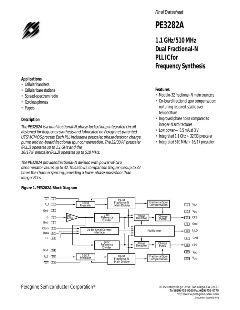
The PE3282A is a dual fractional-N phase-locked loop integrated circuit
designed for frequency synthesis and fabricated on Peregrine’s patented
UTSi® CMOS process. Each PLL includes a prescaler, phase detector, charge
pump and on-board fractional spur compensation. The 32/33 RF prescaler
(PLL1) operates up to 1.1 GHz and the
16/17 IF prescaler (PLL2) operates up to 510 MHz.
Features
• Modulo-32 fractional-N main counters
• On-board fractional spur compensation:
no tuning required, stable over
temperature
• Improved phase noise compared to
integer-N architectures
• Low power—8.5 mA at 3 V
• Integrated 1.1 GHz ÷ 32/33 prescaler
• Integrated 510 MHz ÷ 16/17 prescaler
The PE3282A provides fractional-N division with power-of-two
denominator values up to 32. This allows comparison frequencies up to 32
times the channel spacing, providing a lower phase-noise floor than
integer PLLs.
Figure 1. PE3282A Block Diagram
fin1
6
fin1
5
Gnd
7
fr
8
Gnd
9
Clock 11
Data
12
LE
13
19-Bit
Fractional-N
Main Divider
32/33
Prescaler
9-Bit
Reference
Divider
Ref
Amp
Phase
Detector
21-Bit Serial Control
Interface
14
fin2
16
fin2
15
16/17
Prescaler
Peregrine Semiconductor Corporation®
Charge
Pump
Multiplexer
9-Bit
Reference
Divider
Gnd
Fractional Spur
Compensation
Phase
Detector
18-Bit
Fractional-N
Main Divider
Charge
Pump
Fractional Spur
Compensation
1
VDD
2
VDD
3
CP1
4
Gnd
10
foLD
17
Gnd
18
CP2
19
VDD
20
VDD
6175 Nancy Ridge Drive, San Diego, CA 92121
Tel (619) 455-0660 Fax (619) 455-0770
http://www.peregrine-semi.com
Document 70/0002~07B
PE3282A
Figure 2. Pin Configuration TSSOP (JEDEC MO-153-AC)
VDD
1
20
VDD
2
19
VDD
CP1
3
18
CP2
Gnd
4
17
Gnd
fin2
VDD
fin1
5
16
fin1
6
15
fin2
Gnd
7
14
Gnd
fr
8
13
LE
Gnd
9
12
Data
foLD
10
11
Clock
Table 1. PE3282A Pin Description
Pin No.
Pin Name
Type
Description
1
VDD
(Note 1)
Power supply voltage input. Input may range from 2.7 V to 3.6 V. A bypass capacitor should be
placed as close as possible to this pin and be connected directly to the ground plane.
2
VDD
(Note 1)
Same as pin 1.
3
CP1
Output
Internal charge-pump output for PLL1. For connection to a loop filter for driving the input of
an external VCO.
4
Gnd
5
fin1
Input
Prescaler input from the PLL1 (RF) VCO. 1.1 GHz max frequency.
Ground.
6
fin1
Input
1.1 GHz prescaler complementary input. A bypass capacitor should be placed as close as
possible to this pin and be connected directly to the ground plane. Capacitor is optional with
some loss of sensitivity.
7
Gnd
8
fr
9
Gnd
10
foLD
Output
Multiplexed output of the PLL1 and PLL2 main counters or reference counters, Lock Detect
signals, and data out of the shift register. CMOS output (see Table 10, foLD Programming
Truth Table).
11
Clock
Input
CMOS clock input. Serial data for the various counters is clocked in on the rising edge into the
21-bit shift register. A pull-down resistor is recommended.
12
Data
Input
Binary serial data input. CMOS input data entered MSB first. The two LSBs are the control bits.
A pull-down resistor is recommended.
13
LE
Input
Load Enable CMOS input. When LE is high, data word stored in the 21-bit serial shift register is
loaded into one of the four appropriate latches (as assigned by the control bits). A pull-down
resistor is recommended.
14
Gnd
Ground.
15
fin2
Input
510 MHz prescaler complementary input. A bypass capacitor should be placed as close as
possible to this pin and be connected directly to the ground plane. Capacitor is optional with
some loss of sensitivity.
Input
Prescaler input from the PLL2 (IF) VCO. 510 MHz max frequency.
Ground.
Input
Reference frequency input.
Ground.
16
fin2
17
Gnd
18
CP2
Output
Internal charge-pump output for PLL2. For connection to a loop filter for driving the input of
an external VCO.
19
VDD
(Note 1)
Same as pin 1.
20
VDD
(Note 1)
Same as pin 1.
Ground.
Note 1: VDD pins 1, 2, 19, and 20 are connected by diodes and must be supplied with the same voltage level.
2
Document 70/0002~07B
1.1 GHz/510 MHz Dual PLL IC
Ratings and Operating Ranges
Table 2. Absolute Maximum Ratings
Symbol
Parameter/Conditions
Min
Max
Unit
VDD
Supply voltage
–0.3
4.0
V
VI
Voltage on any input
–0.3
VDD + 0.3
V
II
DC into any input or output
–10
+10
mA
Tstg
Storage temperature range
–65
150
°C
Table 3. Operating Ranges
Symbol
Parameter/Conditions
Min
Max
Unit
VDD
Supply voltage
2.7
3.6
V
TA
Operating ambient temperature range
–40
85
°C
Max
Unit
Table 4. ESD Ratings
Symbol
Parameter/Conditions
Min
VESD
ESD Voltage, Human body model (Note 1)
2000
V
Note 1: Periodically sampled, not 100% tested. Tested per MIL-STD-883, M3015 C2; 2KV.
Electrostatic Discharge (ESD) Precautions
When handling this UTSi device, observe the same precautions that you would use with other ESD-sensitive devices.
Although this device contains circuitry to protect it from damage due to ESD, precautions should be taken to avoid
exceeding the rating specified in Table 4.
Latch-up Avoidance
Unlike conventional CMOS devices, UTSi CMOS devices are immune to latch-up.
Document 70/0002~07B
Peregrine Semiconductor Corporation®
3
PE3282A
Table 5. DC Characteristics
VDD = 3.0 V, –40° C < TA < 85° C, unless specified
Symbol
Parameter
Conditions
IDD
Operational supply current;
PLL1 (RF) enabled
PLL2 (IF) enabled
PLL1 and PLL2 enabled
VDD = 2.7 to 3.6 V
Istby
Min
Typ
Max
Unit
5.5
3.0
8.5
Total standby current
mA
mA
mA
25
mA
Digital inputs: Clock, Data, LE
VIH
High level input voltage
VDD = 2.7 to 3.6 V
VIL
Low level input voltage
VDD = 2.7 to 3.6 V
IIH
High level input current
VIH = VDD = 3.6 V
IIL
Low level input current
VIL = 0, VDD = 3.6 V
0.7 x VDD
V
0.3 x VDD
V
–1
+1
mA
–1
+1
mA
+100
mA
Reference Divider input: fr
IIHR
Input current
VIH = VDD = 3.6 V
IILR
Input current
VIL = 0, VDD = 3.6 V
–100
mA
Digital output: foLD
VOLD
Output voltage LOW
Iout = 1 mA
VOHD
Output voltage HIGH
Iout = –1 mA
0.4
VDD – 0.4
V
V
Charge Pump outputs: CP1, CP2
ICP - Source
Drive current
VCP = VDD/2, TA = 25° C
ICPL
Leakage current
0.5 < VCP < VDD - 0.5 V
ICP - Source
vs.
ICP - Sink
Sink vs. source mismatch
VCP = VDD/2, TA = 25° C
ICP - Sink
ICP vs. TA
Output current vs. temperature
ICP vs. VCP
4
Output current magnitude variation vs.
voltage
–70
mA
70
mA
–5
5
nA
20
%
VCP = VDD/2 + 85° C
–18
%
VCP = VDD/2 - 40° C
+8
%
0.5 < VCP < VDD - 0.5 V,
TA = 25° C
20
%
Document 70/0002~07B
1.1 GHz/510 MHz Dual PLL IC
Table 6. AC Characteristics
VDD = 3.0 V, –40° C < TA < 85° C, unless specified
Symbol
Parameter
Conditions
Min
Max
Unit
10
MHz
Serial Control Interface (see Figure 3)
fClock
Serial data clock frequency
tClockH
Serial clock HIGH time
50
ns
tClockL
Serial clock LOW time
50
ns
tDSU
Data set-up time to Clock rising edge
50
ns
tDHLD
Data hold time after Clock rising edge
10
ns
tLEW
LE pulse width
50
ns
tCLE
Clock falling edge to LE rising edge
50
ns
tLEC
LE falling edge to Clock rising edge
50
ns
tData Out
Data Out delay after Clock falling edge
(foLD pin)
CL = 50 pf
90
ns
Main Divider (Including Prescaler)
fin1
Operating frequency
100
1,100
MHz
fin2
Operating frequency
45
510
MHz
Pfin1
Input level range
External AC coupling
–10
5
dBm
Pfin2
Input level range
External AC coupling
–10
5
dBm
fc
Comparison frequency
10
MHz
50
MHz
Reference Divider
fr
Operating frequency
Vfr
Input sensitivity
External AC coupling
(Note 1)
0.5
VP-P
Note 1: CMOS logic levels may be used if DC coupled.
Document 70/0002~07B
Peregrine Semiconductor Corporation®
5
PE3282A
The PLL1 (RF) VCO frequency fin1 is related to the
reference frequency fr by the following equation:
Functional Description
The Functional Block Diagram in Figure 2 shows a 21bit serial control register, a multiplexed output, and PLL
sections PLL1 and PLL2. Each PLL contains a fractional-N
main counter chain, a reference counter, a phase
detector, and an internal charge pump with on-chip
fractional spur compensation. Each fractional-N main
counter chain includes an internal dual modulus
prescaler, supporting counters and a fractional
accumulator.
fin1 = [(32 x M1) + A1 + (F1/32)] x (fr/R1)
(1) Note that A1 must be less than M1. Also, fin1 must be
greater than or equal to 1024 x (fr/R1) to obtain
contiguous channels.
The PLL2 (IF) VCO frequency fin2 is related to the reference
frequency fr by the following equation:
Serial input data is clocked on the rising edge of Clock,
MSB first. The last two bits are the address bits that
determine the register address. Data is transferred into
the counters as shown in Table 7, PE3282A Register Set. If
the foLD pin is configured as data out, then the contents
of shift register bit S20 are clocked on the falling edge of
Clock onto the foLD pin. This feature allows the PE3282A
and compatible devices to be connected in a daisy-chain
configuration.
fin2 = [(16 x M2) + A2 + (F2/32)] x (fr/R2)
(2) Note that A2 must be less than M2. Also, fin2 must be
greater than or equal to 256 x (fr/R2) to obtain
contiguous channels.
F1 sets PLL1 fractionality. If F1 is an even number,
PE3282A automatically reduces the fraction. For
example, if F1 = 12, then the fraction 12/32 is
automatically reduced to 3/8. In this way, fractional
denominators of 2, 4, 8, 16 and 32 are available. F2 sets
the fractionality for PLL2 in the same manner.
Figure 3. PE3282A Functional Block Diagram
PLL1 (RF)
fin1
A1
5
A1 Counter
0 ð A1 ð 31
M1
9
M1 Counter
3 ð M1 ð 511
Prescaler
32/33
fin1
R1 Counter
3 ð R1 ð 511
fr
F1
5
F1 Counter
0 ð F1 ð 31
C11
R2
C21
9
R2 Counter
3 ð R2 ð 511
Charge
Pump
Phase
Detector
CP1
C12
foLD
Data Out
Multiplexer
Serial Control Interface
PLL2 (IF)
Fractional
Compensation
Phase
Detector
R1
9
Clock
Data
LE
Prescaler
Control Logic
C13
C14
C23
C24
foLD
C22
Charge
Pump
CP2
fin2
fin2
Prescaler
16/17
M2 Counter
3 ð M2 ð 511
F2 Counter
0 ð F2 ð 31
M2
9
A2 Counter
0 ð A2 ð 15
F2
5
Prescaler
Control Logic
Fractional
Compensation
A2
4
6
Document 70/0002~07B
1.1 GHz/510 MHz Dual PLL IC
Table 7. PE3282A Register Set
S20
S19
S18
S17
Reserved
S16
S15
S14
S13
S12
S11
S10
S8
S7
S6
S5
S4
Test PLL2 Synthesizer control
PLL2 Reference counter R2 divide ratio
0
R28
C24
C23
C22
C21
C20
PLL2 Main counter M2 divide ratio
M28 M27 M26 M25 M24 M23 M22 M21 M20 A23
PLL1 Synthesizer control
C14
C13
R27
R26
R25
C12
C11
PLL1 Main counter M1 divide ratio
C10
A22
A21
A20 F24
R23
R22
S2
F23
F22
R18
R17
R16
R15
A13
A12
A11
R14
R13
R12
R21
R20
F21
F20
F13
F12
S0
0
0
Address
0
1
Address
R11
R10
PLL1 Fractional counter F1
numerator value
A10 F14
S1
Address
PLL1 Reference counter R1 divide ratio
PLL1 Swallow counter A1
divide ratio
M18 M17 M16 M15 M14 M13 M12 M11 M10 A14
R24
S3
PLL2 Fractional counter F2
numerator value
PLL2 Swallow
counter A2 divide
ratio
Res.
Reserved
S9
F11
MSB (first in)
F10
1
0
Address
1
1
(last in) LSB
Figure 4. Serial Control Interface Data Timing Diagram
Data
Clock
LE
tDSU
tDHLD
tClockH
tClockL
tLEW
tLEC
tCLE
tData Out
Data Out
(foLD pin)
Document 70/0002~07B
Peregrine Semiconductor Corporation®
7
PE3282A
Table 8. PE3282A Counter Programming Example
Programmable Divide Values
(R1, R2, F1, F2, A1, A2, M1, M2)
Data is clocked into the 21-bit shift register, MSB first.
When LE is asserted HIGH, data is latched into the
registers addressed by the last two bits shifted into the
21-bit shift register, according to Table 7. For example, to
program the PLL1 (RF) swallow counter, A1, the last two
bits shifted into the register (S0 , S1) would be (1, 1). The 5bit A1 counter would then be programmed according to
Table 8. For normal operation, S16 of address (0, 0) (the
Test bit) must be programmed to 0 even if PLL2 (IF) is not
used.
Divide
Value
MSB
LSB
Address
S11
S10
S9
S8
S7
S1
S0
A14
A13
A12
A11
A10
1
1
0
0
0
0
0
0
1
1
1
0
0
0
0
1
1
1
2
0
0
0
1
0
1
1
•
•
•
•
•
•
1
1
31
1
1
1
1
1
1
1
Programmable Modes
Several modes of operation can be programmed with bits C10 - C14 and C20 - C24 , including the phase detector polarity,
charge pump high impedance, output of the foLD pin and power-down modes. The truth table for the programmable
modes is shown in Table 9. The truth table for the foLD output is shown in Table 10.
Table 9. PE3282A Programmable Modes
S15
S14
S13
S12
S11
S1
S0
C24
see
Table 10
C23
see
Table 10
C22
0 = PLL2 CP normal
1 = PLL2 CP High Z
C21 (Note 2)
0 = PLL2 Phase Detector inverted
1 = PLL2 Phase Detector normal
C20 (Note 1)
0 = PLL2 on
1 = PLL2 off
0
0
C14
see
Table 10
C13
see
Table 10
C12
0 = PLL1 CP normal
1 = PLL1 CP High Z
C11 (Note 2)
0 = PLL1 Phase Detector inverted
1 = PLL1 Phase Detector normal
C10 (Note 1)
0 = PLL1 on
1 = PLL1 off
1
0
Note 1: The PLL1 power-down mode disables all of PLL1’s components except the R1 counter and the reference frequency input buffer,
with CP1 (pin 3) and fin1 (pin 5) becoming high impedance. The power down of PLL2 has similar results with CP2 (pin 18) and fin2 (pin
16) becoming high impedance. Power down of both PLL1 and PLL2 further disables counters R1 and R2, the reference frequency input,
and the foLD output, causing fr (pin 8) and foLD (pin 10) to become high impedance. The Serial Control Interface remains active at all
times.
Note 2: The C11 and C21 bits should be set according to the voltage versus frequency slope of the VCO as shown in Figure 4. This
relationship presumes the use of a passive loop filter. If an inverting active loop filter is used the relationship is also inverted.
Figure 5. VCO Characteristics
(1) Positive Slope VCO
• When VCO1 (RF) slope is positive like (1), C11 should be set HIGH.
• When VCO1 (RF) slope is negative like (2), C11 should be set LOW.
• When VCO2 (IF) slope is positive like (1), C21 should be set HIGH.
VCO
Output
Frequency
• When VCO2 (IF) slope is negative like (2), C21 should be set LOW.
(2) Negative Slope VCO
VCO Input Voltage
8
Document 70/0002~07B
1.1 GHz/510 MHz Dual PLL IC
Table 10. foLD Programming Truth Table
X = don’t care condition
foLD
Output State
C14
(PLL1 fo)
C13
(PLL1 LD)
C24
(PLL2 fo)
C23
(PLL2 LD)
Disabled (Note 1)
0
0
0
0
PLL1 Lock detect (Note 2) (LD1)
0
1
0
0
PLL2 Lock detect (Note 2) (LD2)
0
0
0
1
PLL1/PLL2 Lock detect (Note 2)
0
1
0
1
PLL1 Reference divider output (fc1)
1
X
0
0
PLL2 Reference divider output (fc2)
0
X
1
0
PLL1 Programmable divider output (fp1)
1
X
0
1
PLL2 Programmable divider output (fp2)
0
X
1
1
Serial data out
1
0
1
0
Reserved
1
0
1
1
Reserved
1
1
1
0
Counter reset (Note 3)
1
1
1
1
Note 1: When the foLD is disabled the output is a CMOS LOW.
Note 2: Lock detect indicates when the VCO frequency is in “lock”. When PLL1 is in lock and PLL1 lock detect is selected, the foLD pin
will be HIGH, with narrow pulses LOW. When PLL2 is in lock and PLL2 lock detect is selected, the foLD pin will be HIGH, with narrow
pulses LOW. When PLL1/PLL2 lock detect is selected the foLD pin will be HIGH with narrow pulses LOW, only when both PLL1 and PLL2
are in lock.
Note 3: The counter reset state when activated resets all counters. Upon removal of the reset, counters M, A, and F resume counting in
close alignment with the R counter (the maximum error is one prescaler cycle). The reset bits can be activated to allow smooth
acquisition upon powering up.
Document 70/0002~07B
Peregrine Semiconductor Corporation®
9
PE3282A
Phase Comparator Characteristics
PLL1 has the timing relationships shown below for fc1, fp1, LD1, UP1, and DOWN1. When C11 = HIGH, UP1 directs the
internal PLL1 charge pump to source current and DOWN1 directs the PLL1 internal charge pump to sink current. If C11 =
LOW, UP1 and DOWN1 are interchanged.
PLL2 has the timing relationships shown below for fc2, fp2, LD2, UP2, and DOWN2. When C21 = HIGH, UP2 directs the
internal PLL2 charge pump to source current and DOWN2 directs the PLL2 internal charge pump to sink current. If C21 =
LOW, UP2 and DOWN2 are interchanged.
Figure 6. Phase Comparator Timing Diagram
fc1(2)
(Note 1)
fp1(2)
(Note 1)
LD1(2)
(Note 1)
UP1(2)
DOWN1(2)
fc leads fp
fc = fp
fc lags fp
fc lags fp
fc lags fp
Note 1: fc1(2), fp1(2), and LD1(2) are accessible via the foLD pin per programming in Table 10.
10
Document 70/0002~07B
1.1 GHz/510 MHz Dual PLL IC
Figure 7. Typical Application Example
VDD VDD
.01 µF
PLL1 (RF)
OUT
220 pF
220 pF
220 pF
VCO
R2
(Note 1)
C2
VDD VDD
C1
.01 µF .01 µF
VDD
VDD
VDD
VDD
CP1
CP2
Gnd
Gnd
fin1
fin2
fin1
fin2
Gnd
Gnd
R1
(Note 2)
220 pF
1000 pF
Reference
Input
(Note 3)
220 pF
220 pF
.01 µF
1000 pF
VCO
R4
C3
PLL2 (IF)
OUT
(Note 1)
C4
R3
1000 pF
(Note 2)
51K
fr
LE
Gnd
Data
foLD
Clock
51K
51K
foLD
Output
Table 11. PLL1 (RF)
From
Controller
Table 12. PLL2 (IF)
Operating
Conditions
Loop Filter
Values (Note 4)
Operating
Conditions
Loop Filter
Values (Note 4)
fout = 948.075 MHz
R2 = 30 k ohm
fout = 130.45 MHz
R4 = 7.1 k ohm
fref = 14.4 MHz
C2 =.0043 µF
fref = 14.4 MHZ
C4 =.027 µF
fcomp = 800 kHz
C1 = 900 pF
fcomp = 800 kHz
C3 =.0056 µF
Fractionality = 32
Fractionality = 16
Step Size = 25 kHz
Step Size = 50 kHz
ωn = 3.0 kHz
ωn = 2.0 kHz
Phase Margin = 45°
Phase Margin = 45°
N = 1,185 + 3/32
(M = 37, A = 1, F = 3)
N = 163 + 1/16
(M = 10, A = 3, F = 2)
KVCO = 13 MHz/V
KVCO = 5 MHz/V
Kpd = 70 µA/2 ¼ rad
Kpd = 70 µA/2 ¼ rad
Note 1: VCO output assumed to be AC coupled.
Note 2: R1 and R3 are chosen to set the input drive to pins fin1 and fin2. R1 and R3 also allow a larger proportion of the VCO output to be
delivered to the load and attenuate reflected energy from the PLL inputs.
Note 3: The fr input may be DC coupled if driven by an appropriate CMOS level signal. A 50 ohm terminating resistor can be used when
driving the fr pin from an external 50 ohm signal source.
Note 4: The unity gain bandwidth is recommended to be less than or equal to 10 percent of the step size.
Document 70/0002~07B
Peregrine Semiconductor Corporation®
11
PE3282A
Mechanical Information
Figure 8. Package Dimensions: TSSOP (JEDEC MO-153-AC)
1.20 MAX
Seated Height
0.05 MIN
Stand Off
0.60 ±0.15
6.50 ±0.10
20
11
6.40 ±0.30
4.40 ±0.10
Index
1
(dimensions in millimeters)
10
0.65
TYP
12
Document 70/0002~07B
1.1 GHz/510 MHz Dual PLL IC
Ordering Information
Peregrine Semiconductor Corp. standard products are often available in several packages and performance ranges. Part
numbers for ordering the various configurations are defined as follows:
Table 13.Valid ordering number combinations for PE3282A:
Order Code
Part
Marking
Package
Temperature
Shipping
Method
3282-11
PE3282A
20 lead TSSOP
–40 to 85° C
Tube
74 Units/Tube
3282-12
PE3282A
20 lead TSSOP
–40 to 85° C
Tape and Reel
2500 Units/Reel
3282-00
PE3282A-EK
Evaluation Kit
–40 to 85° C
1/Box
Document 70/0002~07B
Peregrine Semiconductor Corporation®
13
Sales Offices
United States
Peregrine Semiconductor Corporation.
6175 Nancy Ridge Drive
San Diego, CA 92121
Tel (619) 455-0660
Fax (619) 455-0770
Data Sheet Identification
Advance Information
The product is in a formative or design stage. The data sheet
contains design target specifications for product development.
Specifications and features may change in any manner without
notice.
Preliminary Specification
The data sheet contains preliminary data. Additional data may
be added at a later date. Peregrine reserves the right to change
specifications at any time without notice in order to supply the
best possible product.
Product Specification
The data sheet contains final data. Peregrine reserves the right
to change specifications at any time without notice in order to
supply the best possible product.
No patent rights or licenses to any circuits described in this
data sheet are implied or granted to any third party.
Peregrine’s products are not designed or intended for use in
devices or systems intended for surgical implant, or in other
applications intended to support or sustain life, or in any
application in which the failure of the Peregrine product could
create a situation in which personal injury or death might
occur. Peregrine assumes no liability for damages, including
consequential or incidental damages, arising out of the use of
its products in such applications.
Peregrine products are protected under one or more of the
following US patents: 5,416,043; 5,600,169; 5,572,040;
5,492,857; 5,663,570; 5,596,205; 5,610,790. Other patents may
be pending or applied for.
The information in this data shee is believed to be reliable.
However, Peregrine assumes no liability for the use of this
information. Use shall be entirely at the user’s own risk. Prices
and specifications are subject to change without notice.
UTSi, the Peregrine logotype, Microcommunicator, SEL Safe, and Peregrine Semiconductor Corporation are registered trademarks of Peregrine Semiconductor Corporation. PE3282A and all PE product
prefixes are trademarks of Peregrine Semiconductor Corporation. Copyright © 1998 Peregrine Semiconductor Corporation. All rights reserved.
Peregrine Semiconductor Corporation®
6175 Nancy Ridge Drive, San Diego, CA 92121
Tel (619) 455-0660 Fax (619) 455-0770
http://www.peregrine-semi.com
Document 70/0002~07B
