Application Note
Understanding
and Performing
USB 2.0 Physical
Layer Testing
Introduction
Engineers involved in the design, characterization and validation of USB 2.0 devices face daily pressures to
speed new products to the marketplace. Tektronix’ comprehensive tool set enables designers to quickly
and accurately perform all compliance tests recommended by the USB-Implementers Forum, Inc. (USB-IF).
Universal Serial Bus (USB 2.0) is a connectivity specification aimed at
peripherals that connect outside the computer in order to eliminate the
hassle of opening the computer case to install cards needed for certain
devices. USB-compliant devices translate into ease-of-use, expandability and speed for the user.
USB 2.0 technology has been widely adopted in today’s marketplace
and introduces a 40 times increase in data rate. This increase in
throughput has now opened the door to a whole host of new peripherals
ranging from full motion video to auxiliary, wallet-sized, hard disk drives.
However, with this tremendous increase in data rate, new levels of test
and measurement challenges arise.
1
www.tektronix.com/usb
The USB 2.0 specification introduces new compliance requirements.
USB 2.0 device designers must properly characterize their designs and
verify compliance to industry standards before device manufacturers
can affix the “certified” USB-IF logo to their packaging. The appropriate
tool set is critical for the performance of USB-IF compliance tests, such
as eye diagram and parametric testing for low-speed, full-speed and
high-speed devices and hubs.
This application note will focus on understanding and performing
USB 2.0 physical layer measurements and electrical compliance testing
(electrical and high-speed tests) and will include a discussion of the
instruments required for each test.
USB 2.0 Physical Layer Testing
Application Note
USB 2.0 Basics
USB 2.0 Electrical Tests
USB 2.0 is a serial bus that utilizes a 4-wire system – VBUS, D-, D+
and Ground. D- and D+ are the prime carriers of the information. VBUS
supplies power to devices that derive their primary power from the
host or hub.
USB 2.0 electrical tests include signal quality, in-rush current check,
and drop and droop tests.
USB 2.0 describes the following speed selections and rise times:
Data Rates
Rise Times
Low Speed (LS)
1.5 Mb/s
75 ns – 300 ns
Full Speed (FS)
12 Mb/s
4 ns – 20 ns
High-Speed (HS)
480 Mb/s
500 ps
USB 2.0 devices can be either self-powered (having their own power
supply) or bus-powered (drawing power through the host). It is
imperative for the self-powered devices to draw as little power as
possible. Tests are outlined in the USB 2.0 specifications for this aspect.
Signal Quality Test
With the advantages of the 40 times increase in data rate comes a
variety of design challenges to vendors of USB 2.0 compliant devices.
Issues of signal quality, such as board layout, jitter, rise and fall times,
EMI, noise, and ground bounce, now rise to the forefront of design
concerns. Maintenance of signal quality is one of the keys to ensure
that a USB 2.0 device is compliant and will be awarded the USB 2.0
certified logo.
The signal quality test includes:
Eye Diagram testing
Signal rate
End of Packet (EOP) width
Cross-over voltage range
Paired JK Jitter
Paired KJ Jitter
Consecutive jitter
Rise time
Fall time
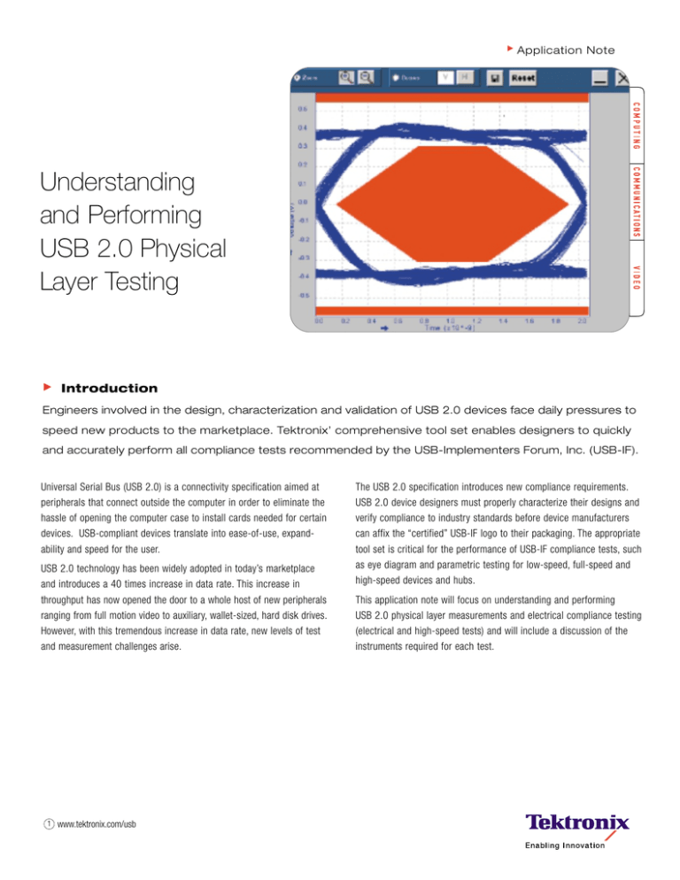
The eye diagram test is unique and the first of its kind for serial data
applications.
The test set-ups for signal quality testing vary for upstream and downstream testing. In the case of upstream testing, signals transmitted from
the device to the host are captured, whereas in the case of downstream
testing, signals transmitted from the host are captured for testing.
Downstream testing is usually performed on ports of a hub.
2
www.tektronix.com/usb
USB 2.0 Physical Layer Testing
Application Note
Figure 2. TDSUSB2 compliance test package running on a TDS7404 DPO.
Figure 1. TDSUSB2 compliance test package running on a TDS7404 DPO.
While performing compliance testing, you need to set up the worstcase USB 2.0 topology scenario to ensure a sufficient test margin.
Devices are tested in the 6th tier to ensure the worst-case scenario.
Further, each hub level is referred to as a tier. The hub-under-test
(HUT) is plugged into the 5th tier so that it operates on the 6th tier.
Test Equipment
Signal quality testing requires a real-time oscilloscope, such as the
TDS7404 digital phosphor oscilloscope (DPO) or TDS694C digital
storage oscilloscope (DSO), and single-ended (low and full speed) and
differential (high speed) probes, like the P6243, P6245 and P6248,
respectively. In addition, this testing requires test software and a test
fixture, such as the TDSUSB2 compliance test package.
Figure 3. Measurement results are automatically displayed using the
TDSUSB2 compliance test package.
Figure 1 shows the operation of the TDSUSB2 compliance test package on a TDS7404 DPO. This test package fully automates the signal
quality test process, allowing designers to perform quick and easy
tests on their designs.
A user must select the measurements to be performed for a particular
signal speed (low, full or high speed). The application must then be
configured based on tier (tier to which the DUT is connected), test
point (test point of the DUT – near or far end), and direction of traffic
(upstream or downstream testing), as shown in Figure 2. After completing these two steps, the user then runs the application.
The test package eliminates the tedium of manual, time-consuming
oscilloscope set-ups, cursor placements and comparison of test results
with USB 2.0 specifications. The results are automatically displayed as
a results summary and details, as illustrated in Figure 3.
www.tektronix.com/usb 3
USB 2.0 Physical Layer Testing
Application Note
Test Equipment
The in-rush current check requires a real-time oscilloscope, such as a
TDS7404 DPO or TDS694C DSO, and current probes, like the TCP202.
This test also requires test software and a test fixture, such as the
TDSUSB2 compliance test package. The TDSUSB2 test package can
be used to automatically set up the oscilloscope for the in-rush current
check. This test package provides direct readout of Charge (uC),
Capacitance (uF) and an automatic indication of pass or fail.
Drop Test
The USB 2.0 specification requires powered USB ports to provide a
VBUS between 4.75 and 5.25 V while bus-powered hubs maintain
a VBUS at 4.4 V or greater. Drop testing evaluates VBUS under both noload and full-load (100 mA or 500 mA, as appropriate) conditions.
Vdrop = Vupstream – Vdownstream
Vupstream = VBUS at hubs upstream
Figure 4. Illustration of a sharp intake of current followed by a comparatively
less steep decay using a TDS694C DSO.
connection
Vdownstream = VBUS at one of hubs
In-Rush Current Check
Because USB 2.0 is a hot-pluggable technology, extreme care is
required to ensure that the current drawn by a device does not exceed
a specified limit. If the current drawn exceeds a specified value, the
operation of other USB 2.0 devices connected to the bus may be hampered. The in-rush current check is performed for both self-powered
and bus-powered devices to verify that the device-under-test (DUT)
does not draw too much current when plugged into the port of a hub.
Typically, one expects a sharp intake of current when a device is
plugged in. This sharp intake of current is followed by a comparatively
less steep decay, as shown in Figure 4. One may observe small humps
or perturbations in the current trace depending on when the device
is reset.
Theoretically, an in-rush current check involves the calculation of
the integral of current over a certain period of time (bounded by the
location of two vertical cursors on the oscilloscope).
The USB 2.0 specification dictates that the total charge drawn by
the device should be less than or equal to 51.5 uC for a VBUS value
of 5.15 V. (The waiver limit for this test is less than 150 uC).
4
www.tektronix.com/usb
downstream port
Bus-powered hubs must have a Vdrop ≤100 mV between their downstream and upstream ports when 100 mA loads are present on their
downstream ports. This requirement ensures that the hubs will supply
4.4 V to a downstream device. Bus-powered devices with Captive
cables must have Vdrop ≤ 350 mV between the upstream connector
and downstream port, including the drop through the cable.
USB 2.0 Physical Layer Testing
Application Note
Test Equipment
USB 2.0 High-speed Tests
Drop tests require a multi-meter. The TDSUSB2 compliance test package
aids in reporting the test results. The multi-meter output for a drop
test can be entered into the TDSUSB2 test package, thus providing
a consolidated report for the user.
Fundamentally, USB 2.0 device compliance tests closely follow the
compliance test protocol for USB 1.1 devices. Primary additions
concern USB 2.0 high-speed mode. High-speed mode adds a new
level of complexity to USB device design. USB 2.0 high-speed tests
include receiver sensitivity, CHIRP, monotonocity and impedance measurement tests.
Droop Test
Vdroop equals the difference in VBUS voltage when a no-load condition
is applied and when a 100 mA load is applied to the port-under-test
(PUT) (all other ports are fully loaded).
The USB 2.0 specification allows a maximum droop of 330 mV. The
droop test evaluates worst-case droop by alternately applying a 100 mA
load and no-load condition to the port under test while all other ports
are supplying the maximum load possible. All VBUS measurements are
relative to local ground.
Test Equipment
Droop tests require a real-time oscilloscope, such as a TDS7404 DPO
or TDS694C DSO, and single-ended probes, like a P6243 or P6245.
In addition, this testing requires test software and a test fixture, such
as the TDSUSB2 compliance test package.
Receiver Sensitivity Test
To increase robust operation in a noisy environment, a USB 2.0 highspeed device must respond to IN* tokens with NAKs* when the signal
level that equals or exceeds the specified level. The test requires
placement of the DUT in Test_SE0_NAK mode. The host is then
replaced by the DG2040 to continue to transmit IN tokens. The signal
amplitude is presented to the DUT at a level at or above 150 mV. At
these levels, the DUT must be in the unsquelched mode, responding
to IN packets with NAKs. The amplitude is then reduced to <100 mV
and at this level, the DUT must be squelched and does not respond to
IN tokens with NAKs.
*Please refer to the USB 2.0 specifications for more information about
IN tokens and NAKs.
The TDSUSB2 test package automatically sets up the oscilloscope for
the desired test configuration. Running the application acquires the
signal, provides the Vdroop measurement, and subsequently provides a
pass or fail indication and detailed measurement results of the test.
www.tektronix.com/usb 5
USB 2.0 Physical Layer Testing
Application Note
Oscilloscope
Test Mode
SW
Chirp K amplitude
Data Generator
Chirp K duration
USB 2.0 Test Fixture
Reset
duration
SMA
HS Device
Chirp Test
Figure 5. Set-up for a receiver sensitivity test using a TDS7404 DPO and
DG2040 data generator.
Figure 6. Test parameters for a CHIRP test.
Test Equipment
CHIRP Test
The receiver sensitivity test requires a real-time oscilloscope, such as
a TDS7404 DPO or TDS694C DSO, and a high-speed data source that
can transmit IN tokens of varying amplitude, such as a DG2040. This
test also requires differential probes, like a P6248, and test software
and a test fixture, such as the TDSUSB2 compliance test package.
The CHIRP test examines the basic timing and voltages of both
upstream and downstream ports during the speed detection protocol.
For a hub, the CHIRP test must be performed on both upstream and
downstream ports.
Figure 5 shows the set-up to perform this test using a TDS7404 DPO
and DG2040 data generator. The TDSUSB2 test package provides
various test set-ups and the test patterns for the DG2040, needed
for receiver sensitivity testing.
To perform CHIRP testing, the DUT is hot-plugged and signaling
is measured with single-ended probes on both data lines. Data is
analyzed for CHIRP K amplitude, CHIRP K duration, Reset duration,
Number of KJ pairs before High Speed termination and delay after
KJKJKJ before device-applied termination.
Figure 6 illustrates various test parameters for the CHIRP test using
a TDS694C DSO.
Test Equipment
The CHIRP test requires a real-time oscilloscope, such as a TDS7404
DPO or TDS694C DSO, with single-ended probes, like a P6243 or
P6245. In addition, this test requires test software and a test fixture,
such as the TDSUSB2 compliance test package.
Manual analysis of the various CHIRP types and conditions is a timeconsuming process. The TDSUSB2 test package automates this process
and automatically documents the results.
6
www.tektronix.com/usb
USB 2.0 Physical Layer Testing
Application Note
Monotonic Signal
Non Monotonic Signal
Figure 7. Illustration of monotonic and non-monotonic USB 2.0 high-speed
signals with a rise time of 500 ps.
High Speed Signal Quality
Equipment Set-up
Tektronix Oscilloscope
with Application Running
Win 2K PC
Figure 9. The monotonicity test set-up uses the high-speed signal quality
test configuration.
Test Equipment
OHCI
Port
Test Mode
Software
B
Recep
Init
Differential Probe
D3
D+ D-
D2
J33
Device
SQ
Test J32
DUT
Vbus
Gnd
Test Fixture
B
pin
Device Under Test
Figure 8. The TDSUSB2 compliance test package captures the test packet
and examines each rising and falling edge for monotonic operation.
Monotonicity Test
When performing a USB 2.0 high-speed compliance test, a developer
needs to verify that the signal under question is monotonic. Monotonicity
verifies that a transmitted signal should smoothly increase or decrease
in amplitude without deviation in the opposite direction. Non-monotonic
signal behavior is caused by metastability, high-frequency noise and
jitter problems in a circuit. Figure 7 compares a monotonic signal with
a non-monotonic signal using a USB 2.0 high-speed signal with a rise
time of 500 ps.
To verify monotonic behavior of a signal, the oscilloscope used should
have a sample rate high enough to capture as many sample points
as possible on a rising or falling edge. In addition, the oscilloscope
should have enough bandwidth to ensure that the high frequency
non-monotonic transition is not attenuated. Hence, an oscilloscope
with a sample rate of 10 GS/s and a bandwidth of 3 or 4 GHz, such
as the TDS694C DSO or TDS7404 DPO, is the ideal tool for monotonicity testing.
Monotonicity testing also requires test software and a test fixture, such
as the TDSUSB2 compliance test package. The monotonicity test for a
USB 2.0 device is verified during test packet examination. The TDSUSB2
compliance test package captures the test packet and examines each
rising and falling edge for monotonic behavior, as shown in Figure 8.
Set-up uses the high-speed signal quality test configuration, as illustrated in Figure 9. The TDSUSB2 compliance test package, coupled
with a high-performance oscilloscope, automates this process and
ensures repeatability of test results.
www.tektronix.com/usb 7
USB 2.0 Physical Layer Testing
Application Note
Test
Equipment
Real-time
Oscilloscope
Signal
Quality
Test
Y
Inrush Droop Receiver CHIRP Impedance
Current Test Sensitivity Test Measurement
Check
Test
Test
Y
Y
Y
Y
Time Domain
Reflectometer
Y
Data Generator
Y
Test Fixture
Y
Y
Y
Y
Y
Test Software
Y
Y
Y
Y
Y
Differential
Probes
Y
Single-ended
Probes
Y
Current Probes
Y
Y
Y
Y
Y
Note: Drop test requires a multi-meter.
Figure 10. TDR measurement made with a TDS8000 digital sampling
oscilloscope coupled with an 80E04 TDR sampling module.
Impedance Measurement Test
Due to the high signal rates of USB 2.0 High-Speed mode, trace and
packaging impedance have become critical parameters. The USB 2.0
High-Speed specification now requires differential impedance measurements of cables, silicon and devices.
The USB 2.0 specification requires that the differential TDR impedance
step response be set to 400 ps. The USB specification defines the
impedance limits referenced from the DUT connector. In general, the
impedance should be between 70 Ohm and 110 Ohm at a given distance from the connector. Cables are also required to meet specific
impedance limits. These limits are 90 Ohm ± 15%.
Test Equipment
The impedance measurement test requires a time domain reflectometer, such as the TDS8000 digital sampling oscilloscope with
80E04 TDR sampling module, which offers unmatched TDR performance on up to eight channels simultaneously.
Figure 10 shows a TDR measurement made with a TDS8000 digital
sampling oscilloscope. The Min and Max measure within the tolerance
specified by the USB differential specification of 90Ω ± 15%.
8
www.tektronix.com/usb
Instrumentation Requirements
for USB 2.0 Physical Layer Testing
The tremendous increase in bit rate afforded by the high-speed data
rate extensions of USB 2.0 opens up a whole new range of USB consumer applications to make the PC a more user friendly and valuable
tool in the workplace and home. With any consumer product opportunity,
time to market is crucial. USB designers are keenly aware that the
correct tool aids in meeting schedule objectives. Especially critical are
the bandwidth, rise time and sample rate of the oscilloscope, along
with the test fixture and fully automatic test software.
USB 2.0 physical layer validation and electrical compliance testing
require a host of test equipment, as the chart above illustrates.
USB 2.0 Physical Layer Testing
Application Note
Effect of Oscilloscope Bandwidth/Rise Time
on Measurement Accuracy
Rise time needs of the oscilloscope depend closely on the rise times of
the signals to be measured. The following empirical formula gives the
relation between measured rise time [RT(measured)], oscilloscope rise
time [RT(oscilloscope)] and signal rise time [RT(signal)];
RT(measured) = [ RT(signal)2 + RT(oscilloscope)2 ]
The following table illustrates the variation of percentage error versus
the ratio of oscilloscope rise time to signal rise time, based on this
relationship.
Rise/Fall Time vs Oscilloscope Bandwidth and Rise Time
Figure 11. TDS7404 digital phosphor oscilloscope.
Selecting Tools for USB 2.0
Physical Layer Testing
Real-Time Oscilloscope
A real-time oscilloscope is the most crucial test instrument for USB 2.0
measurements. When selecting an oscilloscope for these measurements,
it is important to consider the oscilloscope’s rise time, bandwidth and
sample rate. The following section deals with the required performance
characteristics of the real-time oscilloscope.
Bandwidth (GHz)
Rise Time (ps)
Measured Rise Time*
% Error
4
100
509
1.80%
3
120
514
2.80%
2
180
531
6.20%
1
340
604
21%
1
400
640
28%
* Based on a signal with a 500 ps rise time.
When the oscilloscope rise time specification is five times that of the
signal, the error decreases to 1.8%. However, lower oscilloscope rise
times would signify higher error in measurements with respect to signals.
Therefore, in order to measure a signal with a rise time of 500 ps, the
oscilloscope used should ideally have a rise time of 100-120 ps, like a
TDS7404 DPO or TDS694C DSO.
www.tektronix.com/usb 9
USB 2.0 Physical Layer Testing
Application Note
Effect of Oscilloscope Sample Rate on Testing
To capture information at edge speeds as fast as 500 ps, you need at
least 10 sample points on an edge. This requirement becomes even
more important when performing a monotonicity test, mandatory for
high-speed testing.
Tektronix Solutions
In order to have 10 sample points on a 500 ps edge, the oscilloscope
should have a sample rate of at least 20 GS/s.
The TDS694C digital storage oscilloscope (DSO) provides the USB 2.0
device designer with a solution for digital design characterization and
debug. This four-channel oscilloscope employs 3 GHz bandwidth and
10 GS/s per channel real-time sample rate to verify design margins,
characterize setup-and-hold times and measure data jitter on the
USB differential data bus. The TDS694C offers 29 automatic measurements, with measurement statistics, to simplify design verification
and characterization.
Time Domain Reflectometer
The following chart lists various Tektronix real-time oscilloscopes.
Specification
Rise/Fall Time
TDS7404
TDS694C
TDS7254
100 ps
120 ps
160 ps
1.8%
2.80%
4.80%
20 GS/s
10 GS/s
20 GS/s
% Error
Sample Rate
Note: USB 2.0 can encounter edge rates as fast as 500 ps.
The TDS7404 digital phosphor oscilloscope (DPO) is the highest performance member of the TDS7000 Series Windows-based oscilloscopes.
With 20 GS/s maximum real-time sample rate and 4 GHz bandwidth,
the four-channel TDS7404 is the gold standard for high-performance
solutions for verification, debug and characterization of USB 2.0
designs. This instrument features exceptional signal acquisition performance, operational simplicity and open connectivity to the design
environment. The TDS7404 delivers more than 400,000 wfms/s waveform capture rate, enabled by proprietary DPX™ acquisition technology,
to detect and capture elusive events with confidence and ease.
10
www.tektronix.com/usb
A time domain reflectometer is required for the impedance measurement test. The TDS8000 digital sampling oscilloscope with 80E04 TDR
sampling module provides true differential time domain reflectometry
(TDR), making it an ideal solution for USB 2.0 device and cable impedance measurements. This oscilloscope and sampling module can display
both the individual positive and negative TDR waveforms of differential
line characteristics and directly measure the impedance of each conductor or common mode voltage of the differential line. This test system can
also display the true differential measurements of both these lines and
display the impedance in the unit of ohms, providing the user with the
required measurements to validate any USB 2.0 device.
Signal Source
A signal source is required for the receiver sensitivity test. The DG2040
is a 1.1 GHz low jitter data generator that is easily programmed to
output compliant USB 2.0 high-speed data. The two-channel output
permits non-standard differential signaling used by USB devices.
USB 2.0 Physical Layer Testing
Application Note
Fully Automatic Test Software
Fully automatic test software, such as the TDSUSB2 compliance test
package, substantially improves test efficiency by providing automatic
oscilloscope set-ups, automated high-speed tests and quick “onetouch” testing. This test package drastically reduces the test time and
chances of any erroneous measurements.
Semi-Automated Test Software
As the name implies, this kind of solution automates certain tests but
invariably omits certain requirements of compliance testing, resulting
in reduced overall throughput.
Figure 12. Test fixture.
Test Fixture
The test fixture is the most crucial component that enables probing
for every test set-up. The ideal test fixture should provide access to
the differential data lines (D+, D- and VBUS) and offer access/connections via on-board USB connectors or wired dongles.
For receiver sensitivity testing, SMA cables are needed to connect
the data generator to data lines to stimulate the device. Cable access
is also needed to allow impedance measurements by a TDR measurement device.
The TDSUSB2 test package offers a comprehensive compliance test
fixture to enable USB 2.0 testing, as shown in Figure 12.
Test Software
A user may choose among fully automatic test software, semi-automated
test software and manual testing.
Examples of some tests that still need to be manually performed are
high-speed compliance tests such as receiver sensitivity, CHIRP and
monotonicity tests, as well as rise and fall time calculations.
Manual Testing
Traditionally, developers have been using MATLAB scripts to perform
compliance testing. While using the MATLAB scripts, the user must
perform the entire test process manually, which includes setting up
the oscilloscope, placing cursors accurately, storing the captured
signal as a .tsv file, and running MATLAB scripts.
The complexity of the tests and setups demands a phenomenal amount
of expertise from the test engineer. Setting up the oscilloscope is the
most tedious and time-consuming task, as oscilloscope setups differ
for various test configurations. A user is compelled to make continuous
references to exhaustive documentation about test procedures, making
testing difficult and significantly reducing efficiency.
Probes
Probes are a critical component of the measurement system to perform various USB 2.0 compliance tests. Tektronix offers differential
(P6248), single-ended (P6243, P6245) and current (TCP202) probes
that allow access to high-density boards with fine-pitch, hard-to-reach
components while maintaining maximum signal fidelity.
www.tektronix.com/usb 11
USB 2.0 Physical Layer Testing
Application Note
Conclusion
USB 2.0 technology introduced a 40 times increase in data rates
that offers the device designer a migration path for high-performance
peripherals that preserve the ease-of-use consumers have come to
demand. However, this tremendous increase in data rates also presents
new design challenges that the device designer must resolve.
Tektronix offers a comprehensive tool set – sophisticated oscilloscopes,
true differential TDR, high-speed data generator, industry-leading
probes and a fully automated compliance test package – to enable
USB 2.0 device designers to perform quick and accurate electrical
compliance testing and physical layer validation of their designs.
Collectively, this tool set provides superior performance with unparalleled
ease-of-use, making it an ideal solution for USB 2.0 measurements.
Contact Tektronix
ASEAN Countries (65) 356-3900
Austria, Central Eastern Europe, Greece,
Turkey, Malta & Cyprus +43 2236 8092 0
Belgium +32 (2) 715 89 70
Brazil and South America 55 (11) 3741-8360
Canada 1 (800) 661-5625
Denmark +45 44 850 700
Finland +358 (9) 4783 400
France & North Africa +33 1 69 86 81 81
Germany +49 (221) 94 77 400
Hong Kong (852) 2585-6688
India (91) 80-2275577
Tektronix maintains a complete library of updated resources for the
USB device designer at www.tektronix.com/usb.
Italy +39 (02) 25086 501
Japan (Sony/Tektronix Corporation) 81 (3) 3448-3111
Mexico, Central America & Caribbean 52 (5) 666-6333
The Netherlands +31 23 56 95555
Norway +47 22 07 07 00
People’s Republic of China 86 (10) 6235 1230
Poland (48) 22 521 5340
Republic of Korea 82 (2) 528-5299
South Africa +27 11 254-8360
Spain & Portugal +34 91 372 6000
Sweden +46 8 477 65 00
Taiwan 886 (2) 2722-9622
United Kingdom & Eire +44 (0)1344 392000
USA 1 (800) 426-2200
For other areas, contact: Tektronix, Inc. at 1 (503) 627-7111
For Further Information
Tektronix maintains a comprehensive, constantly expanding collection of
application notes, technical briefs and other resources to help engineers
working on the cutting edge of technology.
Please visit “Resources For You” on our Web site at www.tektronix.com
12
www.tektronix.com/usb
Copyright © 2001, Tektronix, Inc. All rights reserved. Tektronix products are covered by U.S. and
foreign patents, issued and pending. Information in this publication supersedes that in all previously
published material. Specification and price change privileges reserved. TEKTRONIX and TEK
are registered trademarks of Tektronix, Inc. All other trade names referenced are the service marks,
trademarks or registered trademarks of their respective companies.
10/01 HMH/PG
55W-15027-0
