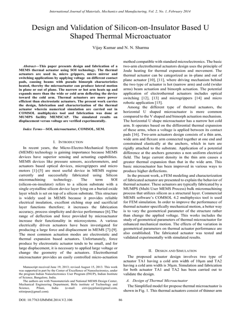
Design and Validation of Silicon-on-Insulator Based U
advertisement

International Journal of Materials, Mechanics and Manufacturing, Vol. 2, No. 1, February 2014 Design and Validation of Silicon-on-Insulator Based U Shaped Thermal Microactuator Vijay Kumar and N. N. Sharma method compatible with standard microelectronics. The basic two-arm electrothermal actuators design uses the principle of Joule heating for thermal expansion and movement. The thermal actuator can be categorized as in–plane and out of plane actuator [10], [11], where driving mechanism behind the two type of actuator is hot (narrow arm) and cold (wider arms) beam actuation and bimorph actuation. The potential application of electrothermal actuators includes optical switching [12], [13] and microgrippers [14] and micro robotic application [15]. Among the different type of thermal actuators, the horizontal U shaped microactuator is more common compared to the V shaped and bimorph actuation mechanism. The horizontal U shape microactuator has a narrow hot cold arm. It operates based on the differential thermal expansion of these arms, when a voltage is applied between its contact pads [16]. Two-arm actuators design consists of a thin arm, wide arm and flexure arm connected together at one end and constrained elastically at the anchors, which in turn are rigidly attached to the substrate. Application of a potential difference at the anchors generates a non uniform electrical field. The large current density in the thin arm causes a greater thermal expansion than that in the wide arm. This basic microactuator has been improved in various ways to produce higher deflections. In the present work, a FEM modeling and characterization of fabricated actuator are presented to explain the behavior of thermal actuator. These actuators are typically fabricated by a MUMPS (Multi User MEMS Process) bulk micromachining process that utilizes silicon as a structural layer. Commercial MEMS software’s COMSOL 4.2 multiphysics tool is used for FEM simulation. In order to improve the performance of thermal actuator specifically mechanical motion, a better way is to vary the geometrical parameter of the structure rather than change the applied voltage. This works includes the study of geometrical parameters of thermal microactuator for enhanced mechanical motion. The effects of the variation in geometrical parameters on thermal actuator performance are also established. The fabricated actuator was tested and validated experimentally with simulated results. Abstract—This paper presents design and fabrication of a MEMS thermal actuator using SOI technology. The thermal actuators are used in, micro grippers, micro mirror and switching applications by applying voltage on different contact pads, causing beams with pseudo bimorph characteristics heated, thereby the microactuator can produce lateral motion in plane or out of plane. The narrow or hot arm heats up and expands more than the wide or cold arm deflecting the device toward the cold arm. Thermal actuators are more power efficient than electrostatic actuators. The present work carries the design, fabrication and characterization of the thermal actuator wherein numerical simulation are carried out in COMSOL multiphysics tool and fabrication was done at MUMPS facility MEMSCAP. The simulated results on displacement versus voltage are verified experimentally. Index Terms—SOI, microactuator, COMSOL, SEM. I. INTRODUCTION In recent years, the Micro-Electro-Mechanical System (MEMS) technology is gaining importance because MEMS devices have superior sensing and actuating capabilities. MEMS devices like pressure sensors, accelerometers, and actuators based optical devices, microgrippers and micro motors [1]-[5] are most useful device in MEMS regime currently and successfully fabricated using Silicon micromachining technology. The term SOI (silicon-on-insulator) refers to a silicon substrate with a single crystalline silicon device layer lying on a buried oxide layer which is set on top of a silicon substrate. This structure is widely used in MEMS because it provides reliable electrical insulation, excellent etching stop and sacrificial layer functions therefore; it increases the fabrication accuracy, process simplicity and device performance [6].The range of deflection and force provided by microactuator increase their functionality in microsystems. A various electrically driven actuators have been investigated for producing a large force and displacement in MEMS [7]-[9]. The most common actuation modes are electrostatic and thermal expansion based actuators. Unfortunately, force produce by electrostatic actuator tends to be small, and for large displacement, it is necessary to applied large voltage or change the geometry of the actuators. Electrothermal microactuator provides an easily controlled micro-actuation II. DESIGN AND SIMULATION The proposed actuator design involves two type of actuator TA1 having a cold arm width of 10µm and TA2 having a cold arm width is 30µm. Simulation and fabrication for both actuator TA1 and TA2 has been carried out to validate the design. Manuscript received June 19, 2013; revised August 15, 2013. This work was supported in part by the Center of Excellence of Nanoelectronics, under the program Indian Nanoelectronics User Program (INUP), Indian Institute of Science, Bangalore, India. The authors are with Nanomaterials and National MEMS Design Center, Mechanical Engineering Department, Birla institute of Technology and Science, Pilani, India (e-mail: cirivijaypilani@gmail.com, nitinipun@gmail.com). DOI: 10.7763/IJMMM.2014.V2.106 A. Design of Thermal Microactuator The Simplified model for propose thermal microactuator is shown in Fig. 1. This thermal actuators consist of thinner arm 86 International Journal of Materials, Mechanics and Manufacturing, Vol. 2, No. 1, February 2014 is called as the hot arm and the wider arm is called as cold arm where each beam have different dimension same materials is used for actuator beams. In this structure, both cold and hot arms are fixed at anchor one end and another end free to move elsewhere. When voltages are applied along the two probing pads, current is passed through the actuator from anchor to anchor, and the hot arm is heated to higher temperature than the cold arm due to the resistance difference. The temperature difference causes the hot arm to elongate more than the cold arm, thus resulting in lateral actuation toward the cold arm side. The SOI based thermal micro actuator has been design using L-Edit Layout editor tool and device were fabricated from MUMPs foundry. The complete die has the dimensions 500µm × 700µm. The used geometrical parameters and material properties of electrothermal actuators are given in Table I: for TA1 and TA2 respectively. (a) Lh Anchor Wc Anchor Wc Wf Lf Lc Fig. 1. Schematic view of thermal microactuator. TABLE I: MATERIAL PROPERTIES AND DIMENSION FOR THERMAL ACTUATOR. Properties Mechanical Properties Young’s modulus of Silicon[E], Poisson’s ratio Density 170x109[Pa] 0.28 2320[kg/m3] Thermal Properties Thermal conductivity of Silicon, Kp Thermal expansion coefficient, α 146 W/(m*K)] 2.6×10⁻⁶[1/K] Electrical Properties Electrical Conductivity 0.25×10⁴ [s/m] Geometry dimensions (μm) Length of cold Arm Lc Width of cold arm Wc Length of hot Arm Lh Width of hot arm Wh Length of flexure Lf Width of Flexure Wf Length of cold hot arm Lch Width of cold hot arm Wch Gap between arms Ga TA1 200µm 10µm 250µm 3µm 50 µm 3 µm 5 µm 3 µm 5 µm (b) Fig. 2. Displacement distribution (a) TA1 (b) TA2 at 8V. III. FABRICATION OF THERMAL MICROACTUATOR The thermal microactuator was fabricated using SOIMUMPS process techniques. SOIMUMPs process is a simple three mask level SOI patterning and etching process derived from work performed at MEMSCAP. The process begins with 100 mm n-type double-side polished silicon on insulator wafers. These wafers consist of both a 25μm silicon layer, a 1μm oxide layer, and a 400μm substrate layer. A bottom side oxide layer that is slightly thinner than the oxide layer is also present on the bottom side of the substrate layer. The top surface of the silicon layer is doped by depositing a phosphosilicate glass (PSG) layer and annealing at 1050°C for 1 hour in argon. This PSG layer is then removed via wet chemical etching. The first layer in the process is the pad metal. A metal stack 20 nm of chrome and 500 nm of gold are patterned through a liftoff process. The structure of microactuator is pattern in 25µm thick silicon after metallization. DRIE (Deep reactive ion etching) is used for selectively etching of the silicon from the front side. After pattering of the microactuator, a front side protection material is applied during the etching from the back side for realizing the actuator. The wafers are then reversed, and the substrate TA2 200µm 30µm 250µm 3µm 50 µm 3 µm 5 µm 3 µm 5 µ m B. FEM Simulation An electro-thermo-mechanical FEM simulation for the actuator was performed using commercial available software COMSOL4.2. The simulation results have been compared with characterization results in subsequent sections. The material properties listed in Table1 were used to evaluate the characterization result and performance of thermal microactuator. Fig. 2(a) and (b) shows a displacement and temperature distribution at applied potential difference of 8V 87 International Journal of Materials, Mechanics and Manufacturing, Vol. 2, No. 1, February 2014 The simulation results by influence of varying voltage and geometrical dimension of thermal actuator also determined. layer is lithographically patterned from the bottom side. This pattern is then reactive ion etched (RIE) into the bottom side native oxide layer. DRIE silicon etch is subsequently used to etch these features completely through the substrate layer. A wet oxide etch process is then used to remove the oxide layer of 1µm in back of active layer. The front side protection material is then stripped in a dry etch process. This “releases” any mechanical structures in the silicon layer that are located over through-holes defined in the substrate layer. The SEM image of complete fabricated thermal actuator chip shown in Fig. 3. B. Effect of Varying a Voltage It is obvious from Fig. 4(a) that displacement increase with increase in voltage and the trend is exponential. Correspondingly the temperature variation of the two arms of thermal actuator also increases in similar way as shown in Fig. 4(b) at maximum 8V. In Fig. 4, we observe that the maximum displacement at tip of actuator was 2.84µm and temperature observed was 991oC at 8V. Due to the difference in the potential and electric current flows in the two arm and the hot arms gets more heated than the cold arm. Hence, there is a downward deflection. (a) (a) (b) Fig. 4. Voltage versus displacement and temperature (a) TA1 and (b) TA2. (b) Fig. 3. Scanning electron microscope images of complete fabricated chip (a) TA1 (b) TA2. C. Effect of Varying Geometrical Dimensions TABLE II: CASE STUDY FOR THERMAL ACTUATORS Geometry dimensions (µm) Case Study IV. RESULT AND DISCUSSION The thermal Microactuator is designed and fabricated using SOI MUMPS techniques. Both Simulation and characterization results carried out to validate the design. Case1 Case2 Case3 Case4 Case5 Case6 Case7 Case8 Case9 Case10 A. Simulated Results The simulation results are presented in this section. The parameters and material properties used for simulation are shown in Table I. The gap between the hot arm and the cold arm are fixed for this analysis. The Fig. 2(a) shows the displacement and voltage FEM model for given parameter. 88 Lh 100 150 170 200 220 250 270 300 320 350 Lc 50 100 120 150 170 200 220 250 270 300 Wc 10 10 10 10 10 10 10 10 10 10 30 30 30 30 30 30 30 30 30 30 International Journal of Materials, Mechanics and Manufacturing, Vol. 2, No. 1, February 2014 The influences of geometry variation on thermal and mechanical characterization of thermal microactuator are also determined. The used geometry dimensions for this analysis is mentioning in Table II with length variation of actuator and other dimensions are fix. The voltage between hot arm and cold arm and gap between the hot arm and cold arm fix for this analysis. It is obvious from the simulation results that the displacement of thermal actuator increases with increase with length of actuator as in Fig. 5 (a). The temperature also increases with length of actuator but not much deviation as with voltage variation in Fig. 5 (b). The influence of variation in width of cold arm with applied range of voltage also determined. The displacement is increase with respected to cold arm width of thermal actuator with applied voltage as in Fig. 6(a) but no much variation in displacement at constant voltage. It is observed from Fig. 6(b) simulation result of thermal actuator the temperature is independent from the width of cold arms. (a) D. Characterization Result The mechanical characterization of fabricated microactuator carried out using Microsystems analyzer MSA-500 is used for mechanical analysis. Fig. 7(a) shows the experimental setup probing on thermal actuators contact pad for measuring displacement at different range of potential difference. Due to the difference in the potential and electric current flow in the two arms and hot arm gets more heated than the cold arm. It observed from simulation also that as the applied voltage increase, the displacement also increase which can be seen in Fig. 8. (a) For TA1 and (b) TA2 by experimental results. The experimentally measured displacement at 8 volts is 2.72µm which approximate simulated results validate the design. (b) Fig. 5. At 8 volt for TA1 and TA2 (a) length of actuator with displacement distribution (b) length of actuator with temperature distribution. (a) (a) Fig. 7(a). Experimental setup probing arrangement on fabricated thermal actuator. The electrical characterization of fabricated chip was carried out using the DC probe station PM5, Agilent Device Analyzer. The current versus voltage plot in figure 9(a) shows clearly that the current increases with applied voltage and this starts saturating beyond 8 volts and resistance value at 8 volts was found 1.342 K-ohms for TA1 and 1.376 K-ohms for TA2. Again change in resistance value in ohms because no much variation in dimension of actuators. It was seen during characterization that the device fails at around 13 (b) Fig. 6(a). Displacement distribution (b) temperature distribution at applied voltage range for Case6 with different values of WC of thermal actuators. 89 International Journal of Materials, Mechanics and Manufacturing, Vol. 2, No. 1, February 2014 volts as it is clear from Fig. 9 (b). This is attributed to the maximum temperature in thermal actuator becoming hot enough, about 1420oC, that silicon is get softened or melt can cause of device failure. V. CONCLUSION The design analysis, fabrication and characterization of the thermal actuators of U shape are presented in current study. The simulation has been carried out using COMSOL Multiphysics tool. The works gives a comparison of simulation results and characterization results. The influence of geometrical and voltage variation on thermal actuator has been also studied to improve maximum displacement and at lesser maximum temperature. The increase in the displacement of the actuator is verified experimentally after fabrication of the designed actuator. It has been observed that displacement of actuator increases with increase in the width of cold arm and length of actuator. Interestingly, the temperature change is only found with change in applied voltage and geometrical parametric change has insignificant effect on change of temperature of the structure. Due to small change of variation in geometrical parameter will not make much variation in temperature of actuator arm with applied voltage. (a) ACKNOWLEDGMENT The work has been carried out under the NPMASS program. The author’s thanks INUP program (Indian Nanoelectronics User Program) Indian Institute of Science, Bangalore, for their support in providing the fabrication facility. REFERENCES (b) Fig. 8. Displacement distributions with applied voltage (a) TA1 (b) TA2. J. W. Judy, “Microelectromechanical systems (MEMS): Fabrication, design and application,” Journal of Smart Materials and structure, vol. 10, pp. 1115-1134, Nov. 2001. [2] K. R. Cochran, L. Fan, and D. L. Devoe, “Moving reflector type micro optical switch for high–power transfer in MEMS-based safely and arming system,” Journal of Microengineering and Micromechanics, vol. 14, pp. 138-146, Oct. 2004. [3] R. Voicu, R. Muller, and L. Eftime, “Design optimization for an electro-thermal actuated polymeric microgrippers,” Design, Test, Integration & Packaging of MEMS/MOEMS, France, 2008. [4] M. A. Greminger, A. S. Sezen, and B. J. Nelson “Microgrippers with Bi-directional thermal actuators,” in Proc. International Conf. on Intelligent Robots and Systems, Canada, 2005, pp. 1166-1171. [5] J. M. Maloney, D. S. Schreiber, and D. L. devoe, “Large force electrothermal linear micro motors,” Journal of Micromachined and Microengineering, vol. 14, pp. 226-234, Nov. 2003. [6] D. V. Dao, K. Nakamura, T. T. Bui, and S. Sugiyama, “Micro/nano-mechanical sensors and actuators based on SOI-MEMS technology,” Journal of Advanced in natural Science, Nanoscience and Nanotechnology, vol. 1, pp. 1-10, March 2010. [7] Y. J. Lai, J. McDonald, M. Kujath, and T. Hubbard, “Force, deflection and power measurements of toggled microthermal actuators,” Journal of Micromechanics and Microengineering, vol. 14, pp. 94-56, Aug. 2004. [8] J. S. Lee, D. S. W. Park, A. K. Nallani, J. B. Lee, “Sub micron metallic electrothermal actuators,” Journal Micromachined and Microengineering, vol. 15, pp. 322-327, Nov. 2004. [9] A. B. Seng, Z. N. Dahari, O. Sidek, and M. A. Miskam, “Design and analysis of thermal microactuator,” European Journal of Scientific Research, vol. 35, 2008, pp.282-292 [10] W. C. Chen, C. C. Chu, J. Hsieh, and W. L. Fang, “A reliable single-layer out-of-plane micromachined thermal actuator,” Sensor and Actuator A, vol. 103, pp. 48-58, 2003. [11] C. Elbuken, N. Topaloglu, J. P. Huissoon et al., “Modeling and analysis of a 2-DOF bidirectional electrothermal microactuator,” Journal of Microsystems Technology, vol. 15, pp. 713-722, May 2009. [12] H. J. Martin and M. Husak, “Thermal microactuator for optical purpose,” in Proc. International Conf. on Information Technology: Coding and Computing, pp. 137-142, April 2001. [1] (a) (b) Fig. 9 (a). I-V charterstics of fabricated thermal actuator chip (b) breakdown plot of thermal actuator at 13 volts. 90 International Journal of Materials, Mechanics and Manufacturing, Vol. 2, No. 1, February 2014 [13] J. Varona, T. Margarita, J. Alatorre, A. A. Hamoui, “Design and fabrication of a MEMS thermal actuator for 3D optical switching application,” presented at IEEE/LEOS Meeting, July 21-23, 2008. [14] N. Chronis and P. L. Luke, “Electrothermally activated SU-8 microgrippers for single cell manipulation in solution,” Journal of Microelectromechanical System, vol. 14, pp. 1-7, Aug. 2005. [15] Q. Chen, Y. Haddab, and P. Lutz, “Microfabricated bistable module for digital microbotics,” Journal of Micro Nano Mechatronics, vol. 6, pp. 1-12, 2011. [16] H. Guckel, J. Klein, T. Christenson, and K. Skrobis, “Thermo-magnetic metal flexure actuators,” IEEE Technical Digest, Solid State Sensor and Actuator Workshop, pp. 73-75, 1992. Microsensor Group, Central Electronics Engineering Research Institute (CEERI), Rajasthan, India. Mr. Kumar has one International Journal paper and he filed two Indain patent. He presented nine National and International conference papers. His field of interest is design fabrication of MEMS sensor and actuator and Microfluidics Devices. N. N. Sharma received his B.E. degree from the Regional Engineering College, Srinagar, India in 1990, the M.E. degree from the Birla Institute of Technology and Science (BITS), Pilani, India in 1998 in Mechanical engineering, and Ph.D. degree from the Birla Institute of Technology and Science (BITS), Pilani, India in 2004. His Ph.D. thesis concerns the broad area of nanodynamics. Since 1998, he has been a member of the Faculty of Mechanical Engineering, BITS. Prof. Sharma currently involved with various aspects of nanotechnology, and MEMS among which nanoactuators and microactuator are foremost. His research interests also include design and control of robotic manipulators. He is an active member of the Center for Robotics and Intelligent Systems, BITS. He is a reviewer of IEEE Transactions on Systems, Man and Cybernetics papers. Vijay Kumar was born in 1985 at Chandigarh, India. He obtained his M.Sc. degree in Electronics Sc. from Kurukshetra University, Kurukshetra, India in 2008. He is currently pursuing Ph.D. in Mechanical Engineering Department, Birla Institute of Technology and Science, Pilani, India since 2011. His Ph.D. involves the broad area of design and fabrication of Microelectromechanical System (MEMS) based sensor. He has two years experience from July 2008 to July 2010, of design and fabrication of MEMS pressure sensor and micro cantilever, in MEMS and 91


