E3A EVALUATION BOARD USER'S GUIDE
for use with QT300 QProx™ sensor IC
Overview
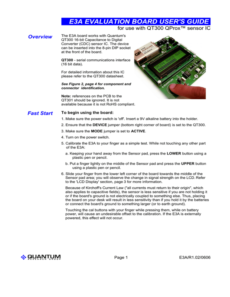
The E3A board works with Quantum's
QT300 16-bit Capacitance to Digital
Converter (CDC) sensor IC. The device
can be inserted into the 8-pin DIP socket
at the front of the board.
QT300 - serial communications interface
(16 bit data).
For detailed information about this IC
please refer to the QT300 datasheet.
See Figure 2, page 4 for component and
connector identification.
Note: references on the PCB to the
QT301 should be ignored. It is not
available because it is not RoHS compliant.
Fast Start
To begin using the board:
1. Make sure the power switch is 'off'. Insert a 9V alkaline battery into the holder.
2. Ensure that the DEVICE jumper (bottom right corner of board) is set to the QT300.
3. Make sure the MODE jumper is set to ACTIVE.
4. Turn on the power switch.
5. Calibrate the E3A to your finger as a simple test. While not touching any other part
of the E3A:
a. Keeping your hand away from the Sensor pad, press the LOWER button using a
plastic pen or pencil.
b. Put a finger lightly on the middle of the Sensor pad and press the UPPER button
using a plastic pen or pencil.
6. Slide your finger from the lower left corner of the board towards the middle of the
Sensor pad area; you will observe the change in signal strength on the LCD. Refer
to the 'LCD Display' section, page 3 for more information.
Because of Kirchoff's Current Law ("all currents must return to their origin", which
also applies to capacitive fields), the sensor is less sensitive if you are not holding it
or if the board's ground is not electrically coupled to something else. Thus, placing
the board on your desk will result in less sensitivity than if you hold it by the batteries
or connect the board's ground to something larger (or to earth ground).
Touching the cal buttons with your finger while pressing them, while on battery
power, will cause an undesirable offset to the calibration. If the E3A is externally
powered, this effect will not occur.
Lq
Page 1
E3A/R1.02/0606
Board
Details
Schematic Diagram
Please refer to the schematic diagram in this guide.
Batteries
Use a 9 Volt Alkaline for best performance.
Remove batteries when using external power!
External Power Connections
!
Connector J1 can be used to power the board. The voltage should be between +8 and
+12 volts DC. Power should be free from switching noise and short-term fluctuations
for best performance.
WARNING: External power - please note! Be sure to remove the batteries first, or
you may cause an explosion and leakage hazard as the batteries will try to charge up
from the external supply!
Device Jumper
Ensure that the jumper is set to the QT300 device (see the note in Overview, page 1
about the nonavailability of the QT301).
Mode Jumper
This jumper allows you to switch the LCD controller to either the ‘active’ or ‘passive’
mode.
Active mode: The LCD controller will drive the QT300 and display the data on the
LCD. To work correctly the QT300 needs to be set to ‘slave’ mode using setups from
a PC (using a QTM300CA board + QT3View software for example).
Passive mode: In this mode the LCD controller ‘sniffs’ data transfers on the SPI lines.
If the E3A is connected to an external host (like a QTM300CA board, or your own host
microcontroller), the LCD will display data as requested by the host.
Sensor Circuit
C1 Capacitor (referred to generically as the Cs or ‘sample’ capacitor) is socketed and
can be replaced for experimentation. Higher values of Cs increase sensitivity, in direct
proportion. Use decent grade capacitors (avoid cheap ceramic capacitors in favor of
plastic film types or at worst, ceramic X7R 5% types for best results). A typical
minimum usable value of Cs is 2nF (0.002uF, or 2,000pF).
'Ext' Sense Connector provides a way to connect the chip to an external sensing
electrode or fluid level probe. The load should have low baseline capacitance (Cx) for
best results. High Cx will decrease apparent sensitivity, perhaps requiring an increase
in Cs to compensate. Shielded cable can be used over limited distances, usually with
an increase in Cs to compensate for the increased Cx loading.
Sensor Select Switch connects the sense pin of the device to either the sense pad or
the external connector. UP = internal pad; DOWN = external connector.
Lq
Page 2
E3A/R1.02/0606
Calibration Switches (Lower, Upper)
QT300: The QT300 requires no calibration; the buttons are only used to calibrate the
LCD bargraph display range between two endpoints (see LCD display below). The
calibration occurs in the display controller microcontroller located under the LCD.
LOWER Switch: Calibrates the lower range endpoint when the electrode is at
minimum load.
UPPER Switch: Calibrates the upper range endpoint when the electrode is loaded.
SPI / CLONE PORT Connector
The pins on this connector are described in Table 1, page 4
This connector is also used to connect the QTM300CA to the E3A for Setups cloning
and to allow QT300 signals to be monitored with QT3View. To use the E3A in this
mode the MODE switch (bottom right corner) must be set to PASSIVE. The LCD
display controller will then ‘sniff’ the data transfers.
LCD
Display
Display Mode
The LCD display shows four different types of information.
On the top line, the LCD displays the raw signal counts (left), the signal deviation in
counts (center) and the signal deviation in percent (right). The bottom line is the signal
deviation bargraph.
The QT300 only sends raw signal data (left). The other numbers and the bargraph are
computed by the E3A’s microcontroller from data recorded during calibration.
Figure 1 LCD Display
Raw Data
16Bits
Delta Signal
(counts)
Delta Signal
(%)
Delta Signal
Bargraph
Lq
Page 3
E3A/R1.02/0606
Figure 2 Board Layout
Spare
Chip (position)
Contrast
Adjust
Power
Terminal
QT300
SPI/Clone
Connector
LCD
Sensor
Select
LCD Controller
Mode Select
External
Electrode
Connector
Calibration
PushButton
Tested Part
Sampling
Capacitor
Part Select
Table 1: J5 - SPI/Clone Port Connector Pinout
Pin
Description
Pin
Description
1
2
3
4
5
n/c
GND
/DRDY
n/c
n/c
6
7
8
9
10
SDO
/REQ
Vcc
SCK
n/c
Table 2 J2 / J3 - Cal Connector Pinouts
Lq
Pin
J2
1
2
3
Analog
GND
PWM
Page 4
Pin
J3
1
2
3
Cal_lower
GND
Cal_upper
E3A/R1.02/0606
Figure 3 Schematic Diagram
Lq
Page 5
E3A/R1.02/0606
lQ
Copyright © 2003-2006 QRG Ltd. All rights reserved.
Patented and patents pending
Corporate Headquarters
1 Mitchell Point
Ensign Way, Hamble SO31 4RF
Great Britain
Tel: +44 (0)23 8056 5600 Fax: +44 (0)23 8045 3939
www.qprox.com
North America
651 Holiday Drive Bldg. 5 / 300
Pittsburgh, PA 15220 USA
Tel: 412-391-7367 Fax: 412-291-1015
This device is covered under one or more United States and corresponding international patents. QRG patent numbers can be found
online at www.qprox.com. Numerous further patents are pending, which may apply to this device or the applications thereof.
The specifications set out in this document are subject to change without notice. All products sold and services supplied by QRG are
subject to our Terms and Conditions of sale and supply of services which are available online at www.qprox.com and are supplied with
every order acknowledgement. QRG trademarks can be found online at www.qprox.com. QRG products are not suitable for medical
(including lifesaving equipment), safety or mission critical applications or other similar purposes. Except as expressly set out in QRG's
Terms and Conditions, no licenses to patents or other intellectual property of QRG (express or implied) are granted by QRG in
connection with the sale of QRG products or provision of QRG services. QRG will not be liable for customer product design and
customers are entirely responsible for their products and applications which incorporate QRG's products.
Developer: Samuel Brunet
