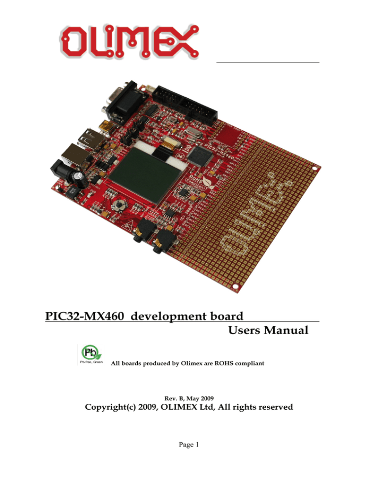
PIC32-MX460 development board
Users Manual
All boards produced by Olimex are ROHS compliant
Rev. B, May 2009
Copyright(c) 2009, OLIMEX Ltd, All rights reserved
Page 1
INTRODUCTION
PIC32-MX460 is low cost development board with the new highperformance 80MHz MIPS-Based 32-bit Flash microcontroller PIC32MX460F512L –
100 pin general purpose and USB. This powerful microcontroller supports various
serial interfaces such as USB Device/Host/OTG, UART. In addition you will find
also audio input and output, debug interface, LCD, UEXT, mini SD/MMC, User
Joystick, User Leds, RF Module area. All this allows you to build a diversity of
powerful applications to be used in a wide range of situations.
BOARD FEATURES
•
PIC32MX460F512L microcontroller
•
Audio input
•
Audio output
•
USB host
•
USB device
•
USB OTG
•
provisions for MRF24J40MA module
•
SD card
•
Reset Circuit
•
Power supply
•
UEXT connector for other Olimex modules like MOD-MP3, MODNRF24Lx, MOD-SMB380, MOD-RFID125 etc.
•
ICSP/ICD connector for programming with PIC-ICD2-POCKET
•
JTAG connector
•
RD232 interface with driver
•
LCD Nokia 3310 BW 84 x48 pixels
•
Quartz crystalls 8 Mhz and 32768 Hz
•
two status LED
•
Joystick
•
Reset button
•
Power plug-in jack with diode bridge can be powered with AC or DC
power supply
•
3.3V voltage regulator
•
Extension slot on every uC pin
•
Gird 100 mils
•
GND bus
•
Vcc bus
•
Four mounting holes 3,3 mm (0,13")
•
PCB: FR-4, 1.5 mm (0,062"), solder mask, silkscreen component print
Page 2
•
Dimensions 135.9x101.6 mm (5.35x4.00")
ELECTROSTATIC WARNING
The PIC32-MX460 board is shipped in protective anti-static packaging. The board
must not be subject to high electrostatic potentials. General practice for working
with static sensitive devices should be applied when working with this board.
BOARD USE REQUIREMENTS
Cables:
Depends on the used programming/debugging tool. It could be 1.8
meter USB A-B cable to connect PIC-ICD2 or PIC-ICD2-POCKET to USB host on PC
or RS232 cable in case of PIC-ICD2-TINY or other programming/debugging tools.
You will need a serial cable if not for programming, than for configuring the board.
You will also need a USB OTG cable.
Hardware:
Programmer/Debugger – most of Olimex programmers are
applicable, for example PIC-ICD2, PIC-ICD2-POCKET, PIC-ICD2-TINY or other
compatible programming/debugging tool.
!!!Warning!!! When you want to program this microcontroller with PIC-ICD2,
PIC-ICD2-POCKET or PIC-ICD2-TINY, before connecting the programmer to your
target board, you should first connect the programmer to your computer and open
MPLAB. There, first from menu Configure – Select Device – choose the
microcontroller you are about to program, then from menu Programmer – Select
Programmer – choose MPLAB ICD 2, wait while MPLAB is downloading operation
system, and after ICD2 is connected – check in menu Programmer – Settings –
Power – there is option – Power target circuit from MPLAB ICD 2 – this option
should be forbidden, you could not select it. Now it is safe to connect the
programmer to your target board.
PROCESSOR FEATURES
PIC32-MX460 board use High-Performance 32-bit RISC microcontroller
PIC32MX460F512L from Microchip Technology Inc with these features:
–
Operating Voltage Range of 2.3V to 3.6V
–
512K Flash Memory (plus an additional 12KB of Boot Flash)
–
32K SRAM Memory
–
Pin-Compatible with Most PIC24/dsPIC® Devices
–
Multiple Power Management Modes
–
Multiple Interrupt Vectors with Individually Programmable Priority
–
Fail-Safe Clock Monitor Mode
–
Configurable Watchdog Timer with On-Chip Low-Power RC Oscillator for
Reliable Operation
Peripheral Features:
–
Atomic SET, CLEAR and INVERT Operation on Select Peripheral Registers
–
Up to 4-Channel Hardware DMA with Automatic Data Size Detection
Page 3
–
USB 2.0 Compliant Full Speed Device and On-The-Go (OTG) Controller
–
USB has a Dedicated DMA Channel
–
40 MHz Crystal Oscillator
–
Internal 8 MHz and 32 kHz Oscillators
–
Separate PLLs for CPU and USB Clocks
–
Two I2C™ Modules
–
Two UART Modules with:
–
RS-232, RS-485 and LIN 1.2 support
–
IrDA® with On-Chip Hardware Encoder and Decoder
–
Parallel Master and Slave Port (PMP/PSP) with 8-bit and 16-bit Data and Up to
16 Address Lines
–
Hardware Real-Time Clock/Calendar (RTCC)
–
Five 16-bit Timers/Counters (two 16-bit pairs combine to create two 32-bit
timers)
–
Five Capture Inputs
–
Five Compare/PWM Outputs
–
Five External Interrupt Pins
–
High-Speed I/O Pins Capable of Toggling at 80 MHz
–
High-Current Sink/Source (18 mA/18 mA) on All I/O Pins
–
Configurable Open-Drain Output on Digital I/O Pins
Debug Features:
–
Two Programming and Debugging Interfaces:
–
2-Wire Interface with Unintrusive Access and Real-time Data Exchange
with Application
–
4-wire MIPS® Standard Enhanced JTAG interface
–
Unintrusive Hardware-Based Instruction Trace
–
IEEE Std 1149.2 Compatible (JTAG) Boundary Scan
Analog Features:
–
16-Channel 10-bit Analog-to-Digital Converter:
–
1000 ksps Conversion Rate
–
Conversion Available During Sleep, Idle
–
Two Analog Comparators
–
5V Tolerant Input Pins (digital pins only)
Page 4
BLOCK DIAGRAM
Page 5
MEMORY MAP
Page 6
SCHEMATIC
C41
100nF
AGND
C43
27k
3
47uF/6.3V/TANT
2
4
6
USB_DEV_DUSB_HOST_DUSB_OTG_D-
+5V
8
7
6
5
L M35 26M-L (SO8 )
VBUSON
Q3
DTC114YKA
HN2x3
1-L
AGND
3.3V
1
R39
10k
R40
U6
MCP130T(NA)
2 VCC RESET 1
3
C27
RSTN
RESET
C28
C29
C30
C31
C32
100nF
100nF
100nF
100nF
100nF
75
65
45
36
15
T 1 107A (6x3.8x2.5 mm )
100nF
3.3VA
VDD
VDD
VDD
VDD
VDD
C34
+
C33
3.3V
30
100nF
1 0uF/6 .3V/T ANT
31
AGND
86
85
+ C35
C36
100nF
100nF C37
C38
VBUS
100nF
RSTN
RST
1 0uF/6 .3V/T ANT
DEBUG INTERFACE:
3.3V
13
R38
11 NC
9
TCK
TMS
7
5
TDO
3
TDI
1
560R
NC
BH14S(PIN<12>-CUT!)
VSS
VSS
VSS
VSS
VSS
25
24
#RF_MODULE_CS 23
22
A_IN
21
VBUSON
20
PGC2
26
PGD2
27
32
33
CS_SD
34
35
41
42
43
44
RB3
RB4
RB6
RB7
RB8
RB9
RB10
RB11
RB12
RB13
RB14
RB15
ICSP
RSTN
PGD2
PGC2
AVDD
AVSS
ENVREG
VCAP/VDDCORE
VUSB
VBUS
TMS/RA0
TCK/RA1
SCL2/RA2
SDA2/RA3
TDI/RA4
TDO/RA5
TRCLK/RA6
TRD3/RA7
PMA7/VREF-/CVREF-/RA9
PMA6/VREF+/CVREF+/RA10
SCL1/INT3/RA14
SDA1/INT4/RA15
PGD1/EMUD1/AN0/CN2/RB0
PGC1/EMUC1/AN1/CN3/RB1
C2IN-/AN2/CN4/RB2
C2IN+/AN3/CN5/RB3
C1IN-/AN4/CN6/RB4
VBUSON/C1IN+/AN5/CN7/RB5
PGC2/EMUC2/AN6/OCFA/RB6
PGD2/EMUD2/AN7/RB7
C1OUT/AN8/RB8
C2OUT/AN9/RB9
CVREFOUT/PMA13/AN10/RB10
PMA12/AN11/RB11
PMA11/AN12/RB12
PMA10/AN13/RB13
PMALH/PMA1/AN14/RB14
PMALL/PMA0/AN15/OCFB/CN12/RB15
Q2
RD2
RD3
RD4
RD5
RD6
RD7
RD8
RD9
RD10
RD11
RD12
CS_UEXT
SCK1
BUT(D)
USB_FAULT
L3
FB0805/600R/200mA(201209-601)
MICRO_AB
GND
C23
C24
39pF
39pF
C25
27pF
C26
27pF
3.3V
R31
33k
#RF_MODULE_RESET
RF_M ODULE_WAKE
#RF_MODULE_CS
MOSI1
MISO1
SCK1
RF_M ODULE_INT
QCT32 768(2x6)/6pF
MOSI1
R32
33k
R34
33k
RF_MODULE
2
R54
5
7
6
4
0R(NA)
0R
VIN
#RESET
WAKE
#CS
SDI
SDO
SCK
INT
3
8
10
NC 9
GND
GND
GND
1
11
12
MRF24J40MA(NA)
CS_UEXT
SCK1
RE0
RE1
RE2
RE3
RE4
RE5
RE6
RE7
RE8
RE9
RF_MODULE_INT
USER JOYSTICK
RF0
RF1
RF2
RF3
#LCD_RES
RXD1
USBID
RXD2
TXD2
TXD1
#CTS2
#RTS2
3.3V
RF8
RF12
RF13
R22
33k
SD_CD
SD_WE
USB_D+
USB_DSCK2
MISO2
MOSI2
RG0
RG1
C58
C59 47pF(NA)
47pF(NA)
RG6
RG7
RG8
RG9
#RF_MODULE_RESET
RG12
RF_MODULE_WAKE
RG13
LCD_D/#C
RG14
#LCD_CS
RG15
R20
33k
BUT(L)
R8
10k
R7
10k
J1
JOYSTICK_MT5_F
R9
33k
BUT(C) R21
330R
BUT(D)
LEFT
LEFT
UP
A<1>
B<4>
CENTER
R10
33k
Common<5>
C<3>
D<6>
DOWN
RA7_BUT(R)
R23
33k
BUT(U)
UP
R24
COMMON
E <2>
Center push
DOWN
330R
BUT(R)
RIGHT
RIGHT
3
PIC32MX460F512L
W U06S
R33
33k
RD15
90
89
57
56
10
11
12
14
96
97
95
1
PMD8/RG0
PMD9/RG1
D+/RG2
D-/RG3
PMA5/SCK2/CN8/RG6
PMA4/SDI2/CN9/RG7
PMA3/SDO2/CN10/RG8
PMA2/#SS2/CN11/RG9
TRD1/RG12
TRD0/RG13
TRD2/RG14
RG15
RD0
MOSI1
LED1
LED2
A_OUT
BUT(L)
RD5_BUT(R)
BUT(U)
BUT(C)
87
88
52
51
49
50
53
40
39
PMD11/RF0
PMD10/RF1
U1RX/RF2
USBID/RF3
PMA9/U2RX/CN17/RF4
PMA8/U2TX/CN18/RF5
U1TX/RF8
#U2CTS/RF12
#U2RTS/BCLK2/RF13
MISO1
Q1
Q8.000MHz/20pF/HC-49SM(SMD)
93
94
98
99
100
3
4
5
18
19
PMD0/RE0
PMD1/RE1
PMD2/RE2
PMD3/RE3
PMD4/RE4
PMD5/RE5
PMD6/RE6
PMD7/RE7
INT1/RE8
INT2/RE9
RC1
RC2
RC3
RC4
MISO1
72
76
77
78
81
82
83
84
68
69
70
71
79
80
47
48
SDO1/OC1/INT0/RD0
OC2/RD1
OC3/RD2
OC4/RD3
PMWR/OC5/CN13/RD4
PMRD/CN14/RD5
PMD14/CN15/RD6
PMD15/CN16/RD7
IC1/RTCC/RD8
IC2/#SS1/RD9
IC3/SCK1/PMCS2/PMA15/RD10
IC4/PMCS1/PMA14/RD11
PMD12/IC5/RD12
PMD13/CN19/RD13
CN20/#U1CTS/RD14
#U1RTS/BCLK1/CN21/RD15
#MCLR
17
38
58
59
60
61
91
92
28
29
66
67
RA7_BUT(R)
RB0
RB1
3.3V
1
2
3
4
5
6
TMS
TCK
SCL2
SDA2
TDI
TDO
RA0
RA1
RA2
RA3
RA4
RA5
RA6
RA7
RA9
RA10
RA14
RA15
TDI,TDO,TMS,TCK
D4
1N58 19(SS 14)
JTAG
14
12
CUT!!! 10
8
6
4
2
55
54
13
6
7
8
9
63
64
73
74
T2CK/RC1
T3CK/RC2
T4CK/RC3
SDI1/T5CK/RC4
OSC1/CLKI/RC12
OSC2/CLKO/RC15
SOSCI/CN1/RC13
SOSCO/T1CK/CN0/RC14
L1
FB080 5/600R/200mA(2012 09-601)
3.3V
100nF
3.3V
U1
2
16
37
46
62
560R
GND
C57
2.2uF
RF MODULE
VDD_E
CLOSE
2
3.3V 3.3V
D5
1N4148
C56
VBUS
DD+
ID
GND
AGND
RESET CIRCUIT
3.3V
USB_OTG
+5V_OTG_PWR
USB_OTG_DUSB_OTG_D+
USBID
3-R
AGND
USB_OTG
2
47uF/6.3V/TANT
SHIELD
USB_A
FB0805/600R/200mA(201209-601)
+5V_OTG_PWR
USB_OTG_DUSB_OTG_D+
HEADPHONES
SCJ325P00XG0B02G
AGND
4
L2
USB
3.3V
3.3V
GND1
GND2
+
100nF
U4
TS4871(SO-8)
2.2uF
1
3
5
C49
C50
AGND
AGND
C51
+
5
8
7
2
C47
R42
33k
USB_D-
10k
33k
#ENA
OUT_A
FLAG_A
IN
FLAG_B
GND
#ENB
OUT_B
C22
4
1
2
3
4
USB_HOST
+5V_HOST_PWR 1
USB_HOST_D2
USB_HOST_D+ 3
100nF
R44
47k
R43
R37
R36
U5
HN2x3
SCJ325P00XG0B02G
AGND
USB_DAGND
C48
470pF
+5V_HOST_PWR
USB_HOST_DUSB_HOST_D+
USB
3-R
AGND
A_OUT
AGND
C46
2.2uF
1
3
5
USB_FAULT
6
1
AGND
USB_D+
USB_D+
1-L
2
AGND
VCC
R41
20k
33nF
USB_HOST
MICROPHONE
47pF
1k
C9
USB_DEV_D+
USB_HOST_D+
USB_OTG_D+
SHIELD
USB_B
GND3
GND4
R52
NA
C44
R49
100k
GN D
1k
33nF
2
4
6
1
2
3
4
10nF C52
AGND
C54
R47
20k
AGND
3.3VA
C11
+5V_USB_DEV
+5V_HOST_PWR
+5V_OTG_PW R
+
100nF
4
R46
470k
2
4
6
HN2x3
2
AGND
R35
1
3
5
47uF/6.3V/TANT
3
C42
1uF
R25
VBUS
VBUS
100nF C55
C40
Z2
BZV55C2V4
USB_DEV
+5V_USB_DEV
USB_DEV_DUSB_DEV_D+
10uF /6.3V/T ANT
C39
47pF
C45
R51
10k
6
47pF
Z1
BZV55C2V4
USB_DEVICE
+5V_USB_DEV
USB_DEV_DUSB_DEV_D+
2
7
U3
MCP601-I/SN
R45
560R
A_IN
USB
R50
560R
R48
100k
100nF C53
AUDIO
3.3VA
USB
3.3VA
+
3.3VA
RD5_BUT(R)
1
RA7/RD5
TXD2,RXD2,#RTS2,#CTS2
MOSI1,MISO1,SCK1,CS_UEXT
3.3V
R55
4.7k
3.3V
R56
4.7k
MISO1
UEXT
3.3V
UEXT-1
UEXT-2
UEXT-3
UEXT-4
UEXT-5
UEXT-6
UEXT-7
UEXT-8
UEXT-9
UEXT-10
TXD1
RXD1
SCL2
SDA2
R53
220R/1%
MOSI1
SCK1
CS_UEXT
RS232
3.3V
BH10S
BH10S
BH10S
BH10S
BH10S
BH10S
BH10S
BH10S
BH10S
BH10S
R16
33k
C13
1
100nF
C14
4
100nF
5
SD/MMC
2
3
6
4
5
7
8
1
SCK2
MISO2
R13
100k
R14
100k
R15
100k
L4
CL470nH/0805/1.76R/250mA
C10
+
SD/MMC
CS_SD
MOSI2
C21
TXD2
#RTS2
CD/DAT3/CS
CMD/DI
VSS
VDD
CLK/SCLK
DAT0/DO
DAT1/RES
DAT2/RES
GND15
C12
100nF
3.3V
100k
10k
3.3V
U2PWR
16VCC
3
R11
R12
LCD
3.3V
R17
560R
RXD2
#CTS2
11
10
12
9
R18
560R
R28
33k
U2
C1+
C1-
V+
V-
C2+
6
T1IN
T2IN
R1OUT
R2OUT
#LCD_RES
R19
C2T1OUT
T2OUT
R1IN
R2IN
14
7
PC_RXD
PC_CTS
13
8
PC_TXD
PC_RTS
RS232
NA
PC_CD
PC_RXD
PC_TXD
ST3232(SO16)
1
2
3
4
5
6
7
8
9
G2
NOKIA_3310
USER LEDS
DB9-F
LED1
LED2
LED1
GYX -S D-TC0 805S YC(YE LLOW)
POWER SUPPLY
C1
470uF/16VDC
GND
1N5819(SS14)
3.3V
2
1N5819(SS14)
D3
IN
R4
240R/1%
100nF
10uF/6.3V(NA)
C4
47uF/6.3V/TANT
1
GYX -S D-TC0805SURK(RED)
R5
390R/1%
C6
R6
560R
10uF/6.3V(NA)
2
3.3VA
CLOSE
PWR
C5
100nF
3.3VA_E
OUT
ADJ/GND
C3
C2
3.3V_E
CLOSE
VR2(3.3V)
LM1117IMPX-ADJ
1
1N5819(SS14)
+5V
R1
220R/1%
R2
330R/1%
R3
330R/1%
D1
+5V_OTG_PWR D2
+
ADJ/GND
+
6VAC
9VDC
+
YDJ-1134
+5V_USB_DEV
OUT
C7
C8
47uF/6.3V/TANT
5V
IN
DB104(SMD)
R26
560R
3.3VA
+5V
VR1(5V)
LM1117IMPX-ADJ
G1
PWR_JACK
100nF
GND_
COPYRIGHT(C), 2009
1
http://www.olimex.com
2
AGND
CLOSE
AGND
Page 7
PIC32-MX460
Rev. B
AGND_E
VDD
SCK
SDIN
D/#C
#SCE
GND
VOUT
#RES
PC_RTS
PC_CTS
MICRO
3.3V
+
1uF/16V/TANT
LCD
1
2
3
4
5
6
7
8
G1
47uF/6.3V/TANT
VIN
C20
100nF
R30
33k
SCK2
MOSI2
LCD_D/#C
#LCD_CS
C15
100nF
C16
100nF
2
R29
33k
LED2
GYX -SD-TC0805SGC(GREE N)
R27
560R
BOARD LAYOUT
Page 8
POWER SUPPLY CIRCUIT
PIC32-MX460 can take power from three sources:
-
PWR_JACK where 9V DC, or 6V AC is applied by external power source.
+5V from USB DEV
+5V from USB OTG
The board power consumption is: about 110 mA with all peripherals and
microcontroller running at full speed.
RESET CIRCUIT
PIC32-MX460 reset circuit is made with R39 (10k) pull-up, R40 (560R) serial resistor
and RST button.
CLOCK CIRCUIT
Quartz crystal
8MHz is connected to PIC32MX460F512L
(OSC1/CLKI/RC12) and pin 64 (OSC2/CLKO/RC15).
Quartz crystal 32.768 KHz is connected to PIC32MX460F512L pin 73
(SOSCI/CN1/RC13) and pin 74 (SOSCO/T1CK/CN0/RC14).
JUMPER DESCRIPTION
3.3V_E
Enable 3.3V board digital power supply.
Default state is closed.
3.3VA_E
Enable 3.3V board analog power supply.
Default state is closed.
VDD_E
Enable PIC32MX460F512L power supply.
Default state is closed.
AGND_E
Enable board analog ground.
Default state is closed.
RA7/RD5
Gives user opportunity to select between RD5 and RA7 BUT(R) connection.
Default state is RA7.
Page 9
pin
63
USB_D+, USB-, VBUS
USB_D+
USB_D-
VBUS
DESCRIPTION:
1-2
1-2
1-2
USB_DEVICE is active!
3-4
3-4
3-4
USB_HOST is active!
5-6
5-6
5-6
USB_OTG is active!
Default state is 1-2.
INPUT/OUTPUT
User joystick with name J1 – this is 4 directions plus center button, in the schematic
the joystick four directions switches are connected: UP, DOWN, LEFT, RIGHT and
CENTER - through 33k resistors to 3.3V also RIGHT is connected to
PIC32MX460F512L pins – 92 (TRD3/RA7), when JMP RA7/RD5 is in position RA7
and 82 (PMRD/CN14/RD5), when JMP RA7/RD5 is in position RD5.
Status LED (yellow) with name LED1 connected to PIC32MX460F512L pin 76
(OC2/RD1).
Status LED (green) with name LED2 connected to PIC32MX460F512L pin 77
(OC3/RD2)
Power supply LED (red) with name PWR – indicates that external power source is
applied and board power supply is applied.
Reset button with name RESET, connected to PIC32MX460F512L pin 13 (#MCLR),
ICSP pin 1 and through R38 (560) to JTAG pin 11.
LCD black/white 84x48 pixels
Page 10
EXTERNAL CONNECTORS DESCRIPTION
JTAG
#Pin
Signal Name
#Pin
Signal Name
1
NC
2
GND
3
TDI
4
GND
5
TDO
6
GND
7
TMS
8
GND
9
TCK
10
GND
11
Through R38 to RSTN
12
Removed
13
NC
14
3.3V
ICSP
#Pin
Signal Name
1
RSTN
2
3.3V
3
GND
4
PGD2
5
PGC2
6
NC
PWR JACK
Pin #
Signal Name
1
Power Input
2
GND
Page 11
RS232
Pin #
Signal Name
1
PC_CD
2
PC_RXD
3
PC_TXD
4
NC
5
GND
6
NC
7
PC_RTS
8
PC_CTS
9
NC
UEXT
Pin #
Signal Name
1
3.3V
2
GND
3
TXD1
4
RXD1
5
SCL2
6
SDA2
7
MISO1
8
MOSI1
9
SCK1
10
CS_UEXT
Page 12
USB_DEVICE
Pin #
Signal Name
1
+5V_USB_DEV
2
USB_DEV_D-
3
USB_DEV_D+
4
GND
USB_HOST
Pin #
Signal Name
1
+5V_HOST_PWR
2
USB_HOST_D-
3
USB_HOST_D+
4
GND
USB_OTG
Pin #
Signal Name
1
+5V_OTG_PWR
2
USB_OTG_D-
3
USB_OTG_D+
4
USBID
5
GND
Page 13
MIC
Pin #
Signal Name
1
AGND
2
NC
3
MIC
HEADPHONE
Pin #
Signal Name
1
AGND
2
IN1=IN2
3
IN2=IN1
SD/MMC
Pin #
Signal Name
1
Pull-up
2
CS_SD
3
MOSI2
4
VDD (power supply)
5
SCK2
6
GND
7
MISO2
8
Pull-up
9
Not connected
10
Not connected
11
Not connected
12
Not connected
Page 14
EXT (Proto area)
Pin #
Signal Name
Pin #
Signal Name
1
3.3V
2
3.3V
3
GND
4
GND
5
5V
6
RST
7
RA15
8
RA14
9
RA10
10
RA9
11
RA7
12
RA6
13
RA5
14
RA4
15
RA3
16
RA2
17
RA1
18
RA0
19
RB15
20
RB14
21
RB13
22
RB12
23
RB11
24
RB10
25
RB9
26
RB8
27
RB7
28
RB6
29
RB4
30
RB3
31
RB1
32
RB0
33
RC4
34
RC3
35
RC2
36
RC1
37
RD12
38
RD15
39
RD10
40
RD11
41
RD8
42
RD9
43
RD6
44
RD7
45
RD4
46
RD5
47
RD2
48
RD3
49
RE0
50
RD0
51
RE2
52
RE1
53
RE4
54
RE3
55
RE6
56
RE5
57
RE8
58
RE7
59
RE9
60
RF13
61
RF12
62
RF8
63
RF3
64
RF2
65
RF1
66
RF0
67
RG1
68
RG0
69
RG7
70
RG6
71
RG9
72
RG8
73
RG13
74
RG12
75
RG15
76
RG14
77
3.3VA
78
3.3VA
79
AGND
80
AGND
Page 15
RF_MODULE
Pin # Signal Name
Pin # Signal Name
1
GND
2
#RF_MODULE_RESET
3
RF_MODULE_WAKE
4
RF_MODULE_INT
5
MOSI1
6
SCK1
7
MISO1
8
#RF_MODULE_CS
9
NC
10
3.3V
11
GND
12
GND
SPI
–
Master and Slave Modes Support
–
Four Different Clock Formats
–
Framed SPI Protocol Support
–
User Configurable 8-bit, 16-bit and 32-bit Data Width
–
Separate SPI Data Registers for Receive and Transmit
–
Programmable Interrupt Event on every 8-bit, 16-bit and 32-bit Data Transfer
–
Operation during CPU Sleep and Idle Mode
–
Fast Bit Manipulation using CLR, SET and INV Registers
I2C
The PIC32MX460F512L microcontroller has two I2C interface modules,
denoted as I2C1 and I2C2. Each I2C module has a 2-pin interface: the SCLx pin is
clock and the SDAx pin is data.
Each I2C module ‘I2Cx’ (x = 1 or 2) offers the following key features:
–
I2C Interface Supporting both Master and Slave Operation.
–
I2C Slave Mode Supports 7 and 10-bit Address.
–
I2C Master Mode Supports 7 and 10-bit Address.
–
I2C Port allows Bidirectional Transfers between Master and Slaves.
–
Serial Clock Synchronization for I2C Port can be used as a Handshake
Mechanism to Suspend and Resume Serial Transfer (SCLREL control).
–
I2C Supports Multi-master Operation; Detects Bus Collision and Arbitrates
Accordingly.
–
Provides Support for Address Bit Masking.
Page 16
MECHANICAL DIMENSIONS
All measures are in Inches.
Page 17
AVAILABLE DEMO SOFTWARE
–
PIC32-MX460 Demo software - includes Audio demo, USB device demo. LCD/joystick demo
Page 18
ORDER CODE
PIC32-MX460 - completely assembled and tested.
How to order?
You can order to us directly or by any of our distributors.
Check our web www.olimex.com/dev for more info.
Revision history:
REV. B - create May 2009
REV.C
February 2011 – change picture
Page 19
Disclaimer:
© 2009 Olimex Ltd. All rights reserved. Olimex®, logo and combinations thereof, are registered trademarks of
Olimex Ltd. Other terms and product names may be trademarks of others.
The information in this document is provided in connection with Olimex products. No license, express or implied
or otherwise, to any intellectual property right is granted by this document or in connection with the sale of
Olimex products.
Neither the whole nor any part of the information contained in or the product described in this document may be
adapted or reproduced in any material from except with the prior written permission of the copyright holder.
The product described in this document is subject to continuous development and improvements. All particulars
of the product and its use contained in this document are given by OLIMEX in good faith. However all warranties
implied or expressed including but not limited to implied warranties of merchantability or fitness for purpose are
excluded.
This document is intended only to assist the reader in the use of the product. OLIMEX Ltd. shall not be liable for
any loss or damage arising from the use of any information in this document or any error or omission in such
information or any incorrect use of the product.
Page 20


