Exclusive Technology Feature
ISSUE: June 2013
New Twist On The Half-Bridge Converter Solves Subtle Failure Mode
by Dennis Feucht, Innovatia Laboratories, Cayo, Belize
The half-bridge circuit is a familiar power circuit but it has a subtle transformer-related failure mode that can be
avoided if understood. If you know what a half-bridge circuit is, it might not be the failure mode you think it is.
The familiar problem arises from capacitors on the primary side of the circuit forming a resonance with the
primary inductance, resulting in both flux and charge imbalance. A lesser-known difficulty arises from a
resonance on the secondary side of the circuit where the secondary leakage inductance resonates with the
diodes’ parasitic capacitance, leading to excessive voltage overshoot and power dissipation. This article explains
how this failure mode arises and how to avoid it through a reconfiguration of the secondary-side circuit.
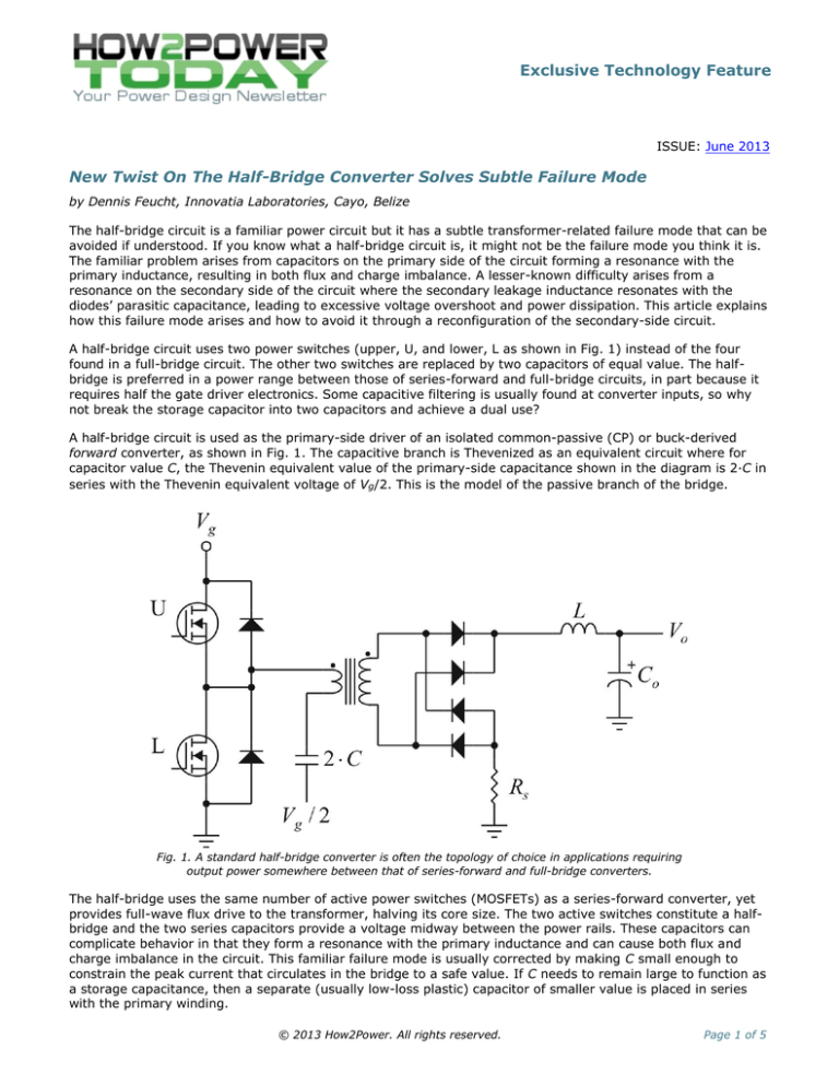
A half-bridge circuit uses two power switches (upper, U, and lower, L as shown in Fig. 1) instead of the four
found in a full-bridge circuit. The other two switches are replaced by two capacitors of equal value. The halfbridge is preferred in a power range between those of series-forward and full-bridge circuits, in part because it
requires half the gate driver electronics. Some capacitive filtering is usually found at converter inputs, so why
not break the storage capacitor into two capacitors and achieve a dual use?
A half-bridge circuit is used as the primary-side driver of an isolated common-passive (CP) or buck-derived
forward converter, as shown in Fig. 1. The capacitive branch is Thevenized as an equivalent circuit where for
capacitor value C, the Thevenin equivalent value of the primary-side capacitance shown in the diagram is 2·C in
series with the Thevenin equivalent voltage of Vg/2. This is the model of the passive branch of the bridge.
Fig. 1. A standard half-bridge converter is often the topology of choice in applications requiring
output power somewhere between that of series-forward and full-bridge converters.
The half-bridge uses the same number of active power switches (MOSFETs) as a series-forward converter, yet
provides full-wave flux drive to the transformer, halving its core size. The two active switches constitute a halfbridge and the two series capacitors provide a voltage midway between the power rails. These capacitors can
complicate behavior in that they form a resonance with the primary inductance and can cause both flux and
charge imbalance in the circuit. This familiar failure mode is usually corrected by making C small enough to
constrain the peak current that circulates in the bridge to a safe value. If C needs to remain large to function as
a storage capacitance, then a separate (usually low-loss plastic) capacitor of smaller value is placed in series
with the primary winding.
© 2013 How2Power. All rights reserved.
Page 1 of 5
Exclusive Technology Feature
This article explains a different complication involving the transformer secondary currents. It involves a
secondary-circuit resonance that is also associated with the transformer, with its secondary leakage inductance.
Despite this problem, an elegant solution described in this article can transform the half-bridge circuit into one
of the most attractive and reliable converter topologies.
Half-Bridge Behavior
On successive half-cycles of the drive (corresponding to the on-times of switches U and L), the transformer flux
is driven with opposing polarities, resulting in full core utilization. A full-wave diode bridge circuit also allows full
utilization of the transformer secondary winding, delivering power to the output on both half-cycles. The diode
bridge drives an inductor followed by a capacitor, which develops an output voltage Vo across it.
The full switching cycle starts when switch U turns on, starting time interval ton+. A voltage of Vg/2 is applied to
the primary winding and current quickly ramps up across the leakage inductance, delivering secondary current,
as shown below in Fig. 2. When vs > Vo, the top and bottom diodes conduct and the inductor current, iL, ramps
up.
Fig. 2. Secondary-side current flow at the beginning of switching cycle when the upper MOSFET in
the half bridge turns on.
When switch U turns off, starting toff+, the primary winding is clamped by the diode shunting switch L. This
causes vs to reverse polarity, and the transferred current quickly ramps down as the primary winding voltage
opposes it across the leakage inductance. The primary magnetizing current, imp, concurrently transfers to the
secondary (as ims = nimp, shown below in Fig. 3. in blue), where it is opposed by Vo and decreases.
Fig. 3. Secondary-side current flow when the upper MOSFET turns off.
The output or load current is iL. If ims < iL, ims is then part of the inductor current. The remaining iL flows
through bridge diodes as clamp current (in red). Only the top diode is off because vs opposes its conduction.
If ims decreases to zero during the off-time, then vs collapses to zero and all four bridge diodes conduct, as
shown in Fig 4.
© 2013 How2Power. All rights reserved.
Page 2 of 5
Exclusive Technology Feature
Fig. 4. Secondary-side current flow when the upper MOSFET is off and the magnetizing current
(ims) decreases to zero.
During off-time, the bridge is shorting the secondary winding while delivering inductor current. The inductor
current splits between the shunt series-diode branches. This short is referred (or “reflected”) back to the
primary winding as 0 V.
For the negative half-cycle, switch L turns on and ton– commences, as shown below. The behavior is
symmetrical with the positive half-cycle.
Fig. 5. Secondary-side current flow when the lower MOSFET turns on.
During toff–, primary current flows in the upper diode shunting switch U. And for ims < iL, ims contributes to iL and
the remaining inductor current flows through the bottom and top diodes so that only the third diode from top is
off. If ims decreases to zero during toff–, then inductor current splits between the diode branches from ground.
When ton+ begins again, the magnetizing current adds to the secondary current, and transfers back to the
primary winding when it changes polarity. As secondary current quickly increases with Vg/2 applied to the
leakage inductance, the secondary clamp diodes begin reverse recovery only when the secondary current
equals iL, causing the clamp-diode current to go to zero. At the time the clamping diodes turn off, the
capacitance at the input-terminal node of the inductor (parasitic capacitance associated with the diodes) has
been discharged by the clamping action to 0 V. Then the full secondary current flows into this capacitance,
charging it and exciting a resonance with the secondary leakage inductance.
This resonance typically requires series RC damping across the secondary winding. It can dissipate excessive
power because the resonance is maximally excited by the release of the shorted secondary winding with a fully
discharged capacitance. The full turn-on voltage referred from the primary is initially applied across the
secondary leakage inductance causing a maximum rate of increase of current in it. It is a bad resonance to
have to damp.
© 2013 How2Power. All rights reserved.
Page 3 of 5
Exclusive Technology Feature
The Half-Bridge Series-L Converter
The secondary resonance problem is solved by swapping the secondary inductor and diode bridge as shown in
Fig. 6. This results in a quite different kind of converter—a half-bridge series-L (HBSL) converter—with zerocurrent switching (ZCS) of the bridge diodes and zero-voltage switching (ZVS) turn-on of the MOSFETs.
Fig. 6. By reversing the order of the diode bridge and the inductor on the secondary side, the
half-bridge series L converter eliminates the secondary resonance problem that can occur in
conventional half-bridge converter designs.
The transformer secondary leakage inductance, Lls, is now in series with the external L and is negligible; the
total inductance is now
Lc = Lls + L.
This inductance can also resonate with the input capacitance of the bridge but is much larger. The resonant
impedance,
Zn
Lc
Cd
is hence much larger and might be envisioned as being damped as a parallel resonance by the RcCc damper
shown in the Fig. 6 circuit. However, the damper is not needed because of the clamping behavior of the diode
bridge. No ringing can occur at the bridge input node because the diodes connect this node across the output
with a very large Co that reduces any possible resonance to a low frequency with negligible ringing.
This circuit is no longer an isolated common-passive (buck) converter but is very different. One of the
advantages of the new circuit, other than solving the secondary resonance problem by diode clamping is the
zero-power switching of the diode bridge. The original circuit not only required an RC damper with a large
power resistor; the diodes also needed heat sinking. With the above circuit, neither damper nor heat sinks are
required.
The approach taken in this article follows the philosophy “if you can’t fix it, feature it.” The new circuit takes one
of the elements of the problem, the transformer leakage inductance which resonates with the secondary diode
© 2013 How2Power. All rights reserved.
Page 4 of 5
Exclusive Technology Feature
capacitances, and turns the leakage inductance into an advantage. The resonance is modified to become a
desirable if not negligible aspect of the overall behavior. This circuit has been described in detail, with design
equations and procedure, in Eco-Electrical Home Power Electronics, D. Fichte, Elektor (www.elektor.com), 2009
in the “Wind Converter Circuits” chapter.
In the conventional half-bridge converter, by applying tighter magnetic coupling in the transformer, the
secondary resonance problem can be reduced though not avoided entirely. Looser coupling is characteristic of
transformers with turns ratios far from one. For example, in a 750-W capacitor-bank charger for a magnetizer,
with 120-V ac input and a maximum C-bank voltage of 750 V, the required turns ratio of 10 resulted in a clear
manifestation of the problems described previously. By interleaving the primary and secondary windings, the
coupling can be increased though at added expense.
Use of the HBSL converter is an effective solution. Its major disadvantage is that L has a bipolar current
waveform and requires ferrite instead of the lower-cost iron-powder core material. However, when designed
correctly, L provides inherent short-circuit protection at the output.
About The Author
Dennis Feucht has been involved in power electronics for 25 years, designing motordrives and power converters. He has an instrument background from Tektronix, where
he designed test and measurement equipment and did research in Tek Labs. He has
lately been doing current-loop converter modeling and converter optimization.
For more on magnetics design, see the How2Power Design Guide, select the Advanced Search option, go to
Search by Design Guide Category, and select “Magnetics” in the Design Area category.
© 2013 How2Power. All rights reserved.
Page 5 of 5
