Product Specification
PE33241
UltraCMOS® Integer-N PLL Frequency
Synthesizer for Low Phase Noise
Applications
Peregrine’s PE33241 is a high-performance Integer-N
PLL capable of frequency synthesis up to 5 GHz. This
device is designed for use in industrial and military
applications, point-to-point radios, wireless infrastructure
and CATV equipment.
Frequency range
5 GHz in 10/11 prescaler modulus
4 GHz in 5/6 prescaler modulus
Phase noise floor figure of merit:
-230 dBc/Hz
Low power: 75 mA typ @ 2.8V
Selectable prescaler modulus of 5/6 or
10/11
Serial or direct mode access
Internal phase detector
Packaged in a 48-lead 7x7 mm QFN
LE
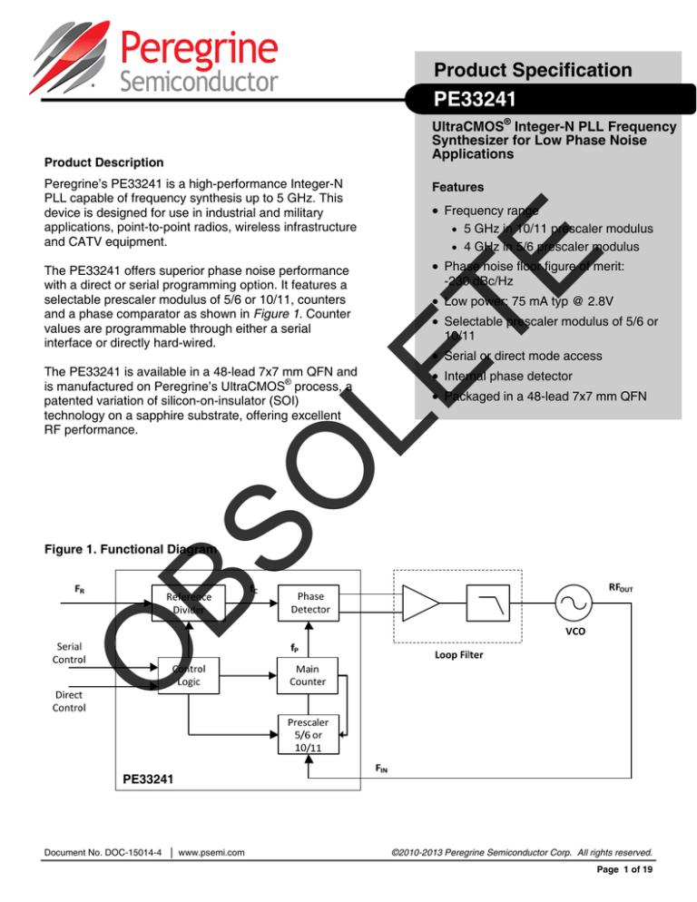
The PE33241 offers superior phase noise performance
with a direct or serial programming option. It features a
selectable prescaler modulus of 5/6 or 10/11, counters
and a phase comparator as shown in Figure 1. Counter
values are programmable through either a serial
interface or directly hard-wired.
Features
TE
Product Description
BS
O
The PE33241 is available in a 48-lead 7x7 mm QFN and
is manufactured on Peregrine’s UltraCMOS® process, a
patented variation of silicon-on-insulator (SOI)
technology on a sapphire substrate, offering excellent
RF performance.
O
Figure 1. Functional Diagram
PE33241
Document No. DOC-15014-4 │ www.psemi.com
©2010-2013 Peregrine Semiconductor Corp. All rights reserved.
Page 1 of 19
PE33241
Product Specification
Figure 2. Pin Configurations (Top View)
Figure 3. Package Type
48-lead 7x7 mm QFN
Table 1. Pin Descriptions
LE
TE
Pin 1 dot
marking
Pin Name
Interface Mode
Type
1
VDD
Both
Note 1
Description
O
Pin #
Power supply input. Input may range from 2.65V to 2.95V. Bypassing recommended
R4
Direct
Input
R counter bit 4
R5
Direct
Input
R counter bit 5
4
A3
Direct
Input
A counter bit 3
N/C
Both
Note 3
GND
Both
M3
Direct
Input
M counter bit 3
M2
Direct
Input
M counter bit 2
M1
Direct
Input
M counter bit 1
M0
Direct
Input
M counter bit 0
Note 1
5
6
7
8
9
O
10
BS
2
3
No connect
Ground
11
VDD
Both
12
GND
Both
13
M8
Direct
Input
M counter bit 8
14
M7
Direct
Input
M counter bit 7
SCLK
Serial
Input
Serial clock input. SDATA is clocked serially into the 20-bit primary register (E_WR “low”)
or the 8-bit enhancement register (E_WR “high”) on the rising edge of SCLK
M6
Direct
Input
M counter bit 6
SDATA
Serial
Input
Binary serial data input. Input data entered MSB first
M5
Direct
Input
M counter bit 5
S_WR
Serial
Input
Serial load enable input. While S_WR is “low”, SDATA can be serially clocked. Primary
register data is transferred to the secondary register on S_WR rising edge
M4
Direct
Input
M counter bit 4
15
16
17
Power supply input. Input may range from 2.65V to 2.95V. Bypassing recommended
Ground
©2010-2013 Peregrine Semiconductor Corp. All rights reserved.
Page 2 of 19
Document No. DOC-15014-4 │ UltraCMOS® RFIC Solutions
PE33241
Product Specification
Table 1. Pin Descriptions (continued)
Pin #
Pin Name
Interface Mode
18
GND
Both
19
Direct
Direct
Input
Select “high” enables Direct Mode. Select “low” enables Serial Mode
20
A0
Direct
Input
A counter bit 0
E_WR
Serial
Input
Enhancement register write enable. While E_WR is “high”, SDATA can be serially
clocked into the enhancement register on the rising edge of SCLK
Input
A counter bit 1
A counter bit 2
21
Type
Description
Ground
Direct
A2
Direct
Input
23
VDD
Both
Note 1
Power supply input. Input may range from 2.65V to 2.95V. Bypassing recommended
24
N/C
Both
Note 3
No connect
25
Pre_En
Direct
Input
Prescaler enable, active “low”. When “high”, FIN bypasses the prescaler
26
Pre_5/6_Sel
Direct
Input
5/6 modulus select, active “high.” When “low,” 10/11 modulus selected
27
VDD
Both
Note 1
28
—
FIN
Both
Input
Prescaler complementary input. A 22 pF bypass capacitor should be placed as close
as possible to this pin and be connected in series with a 50Ω resistor to ground
29
FIN
Both
Input
Prescaler input from the VCO, 5 GHz max frequency. A 22 pF coupling capacitor
should be placed as close as possible to this pin and be connected in shunt to a
50Ω resistor to ground
30
GND
Both
31
Dout
Serial
32
Cext
Both
Output
Logical “NAND” of PD_D and PD_U terminated through an on chip 2 kΩ series
resistor. Connecting Cext to an external capacitor will low pass filter the input to the
inverting amplifier used for driving LD
33
LD
Both
Output
Lock detect and open drain logical inversion of Cext. When the loop is in lock, LD is
high impedance, otherwise LD is a logic low (“0”)
LE
Power supply input. Input may range from 2.65V to 2.95V. Bypassing recommended
Ground
Data Out. The MSEL signal and the raw prescaler output are available on Dout
through enhancement register programming
O
Output
BS
34
TE
A1
22
VDD
Both
Note 1
Power supply input. Input may range from 2.65V to 2.95V. Bypassing recommended
PD_D
Both
Output
PD_D is pulse down when fp leads fc
PD_U
Both
Output
PD_U is pulse down when fc leads fp
VDD
Both
Note 1
Power supply input. Input may range from 2.65V to 2.95V. Bypassing recommended
VDD
Both
Note 1
Power supply input. Input may range from 2.65V to 2.95V. Bypassing recommended
FR
Both
Input
VDD
Both
Note 1
41
ENH
Serial
Input
42
GND
Both
43
N/C
Both
Note 3
No connect
44
R0
Direct
Input
R counter bit 0
45
R1
Direct
Input
R counter bit 1
46
R2
Direct
Input
R counter bit 2
47
R3
Direct
Input
R counter bit 3
48
GND
Both
35
36
37
38
39
O
40
Reference frequency input
Power supply input. Input may range from 2.65V to 2.95V. Bypassing recommended
Enhancement mode. When asserted low (“0”), enhancement register bits are
functional
Ground
Ground
Notes: 1. VDD pins 1, 11, 23, 27, 34, 37, 38 and 40 are connected by diodes and must be supplied with the same positive voltage level
2. All digital input pins have 70 kΩ pull-down resistors to ground
3. No connect pins can be left open or floating
Document No. DOC-15014-4 │ www.psemi.com
©2010-2013 Peregrine Semiconductor Corp. All rights reserved.
Page 3 of 19
PE33241
Product Specification
Electrostatic Discharge (ESD) Precautions
Table 2. Operating Ranges
Symbol
Min
Typ
Max
Unit
VDD
2.65
2.8
2.95
V
10
dBm
+85
C
Supply voltage
RF input power, CW
50 MHz – 5 GHz
PMAX,CW
Operating ambient
temperature range
-40
TA
+25
Latch-Up Avoidance
Table 3. Absolute Maximum Ratings
Symbol
Min
Max
Unit
VDD
-0.3
3.3
V
Voltage on any input
VI
-0.3
VDD + 0.3
V
DC into any input
II
-10
+10
mA
DC into any output
IO
-10
+10
mA
TST
-65
+150
°C
Supply voltage
Storage temperature range
ESD voltage HBM1
All pins except pin 31
ESD voltage HBM1,2
On pin 31
1000
V
300
V
VESD,HBM
Notes: 1. Human Body Model (MIL-STD 883 Method 3015)
2. Pin 31 is not used in normal operation
Unlike conventional CMOS devices, UltraCMOS®
devices are immune to latch-up.
Moisture Sensitivity Level
The Moisture Sensitivity Level rating for the
PE33241 in the 48-lead 7x7 mm QFN package is
MSL3.
LE
Parameter/Condition
When handling this UltraCMOS® device, observe
the same precautions that you would use with
other ESD-sensitive devices. Although this
device contains circuitry to protect it from
damage due to ESD, precautions should be
taken to avoid exceeding the rating specified.
TE
Parameter/Condition
O
BS
O
Exceeding absolute maximum ratings may cause
permanent damage. Operation should be
restricted to the limits in the Operating Ranges
table. Operation between operating range
maximum and absolute maximum for extended
periods may reduce reliability.
©2010-2013 Peregrine Semiconductor Corp. All rights reserved.
Page 4 of 19
Document No. DOC-15014-4 │ UltraCMOS® RFIC Solutions
PE33241
Product Specification
Table 4. DC Characteristics @ 25°C, VDD = 2.8V, unless otherwise noted
Symbol
IDD
Parameter
Condition
Operational supply current
Min
Typ
Max
Unit
Prescaler disabled,
fc = 50 MHz, FIN = 500 MHz
40
50
mA
5/6 prescaler,
fc = 50 MHz, FIN = 3 GHz
75
100
mA
10/11 prescaler,
fc = 50 MHz, FIN = 3 GHz
76
100
mA
TE
FIN
Digital Inputs: All except FR, FIN, —
VIH
High level input voltage
0.7 x VDD
VIL
Low level input voltage
IIH
High level input current
VIH = VDD = 2.95V
IIL
Low level input current
VIL = 0, VDD = 2.95V
Reference Divider input: FR
High level input current
IILR
Low level input current
Counter and phase detector outputs: PD_D , PD_U
VOLD
Output voltage LOW
VOHD
Output voltage HIGH
Lock detect outputs: Cext, LD
Output voltage LOW, Cext
VOHC
Output voltage HIGH, Cext
VOLLD
Output voltage LOW, LD
Iout = -3 mA
μA
μA
μA
μA
0.4
VDD - 0.4
V
V
0.4
V
0.4
V
VDD - 0.4
V
O
BS
Iout = 1 mA
70
-300
Iout = 100 μA
Iout = -100 μA
V
300
Iout = 6 mA
O
VOLC
VIH = VDD = 2.95V
VIL = 0, VDD = 2.95V
0.3 x VDD
-10
LE
IIHR
V
Document No. DOC-15014-4 │ www.psemi.com
©2010-2013 Peregrine Semiconductor Corp. All rights reserved.
Page 5 of 19
PE33241
Product Specification
Table 5. AC Characteristics @ 25°C, VDD = 2.8V, unless otherwise noted
Symbol
Parameter
Condition
Min
Typical
Max
Unit
10
MHz
fClk
Serial data clock frequency1
tClkH
Serial clock HIGH time
30
ns
tClkL
Serial clock LOW time
30
ns
tDSU
SDATA set-up time after SCLK rising edge
10
ns
tDHLD
SDATA hold time after SCLK rising edge
10
ns
TE
Control interface and latches (see Figures 14 and 15)
30
ns
30
ns
30
ns
30
ns
30
ns
tPW
S_WR pulse width
tCWR
SCLK rising edge to S_WR rising edge
tCE
SCLK falling edge to E_WR transition
S_WR falling edge to SCLK rising edge
tWRC
tEC
E_WR transition to SCLK rising edge
tMDO
Main divider 10/11 (including prescaler)
FIN
Operating frequency
PF IN
Input sensitivity
External AC coupling
800 MHz – < 4 GHz
4 GHz – 5 GHz
PF IN
Input sensitivity
Main divider (prescaler bypassed)
FIN
External AC coupling
800 MHz – 4 GHz
BS
PF IN
Operating frequency
-102
-52
800
O
Operating frequency
8
800
Main divider 5/6 (including prescaler)
FIN
CL = 12 pF
LE
MSEL data out delay after FIN rising edge
Input sensitivity
-102
50
External AC coupling
50 MHz – 800 MHz
-152
ns
5000
MHz
-5
0
dBm
dBm
4000
MHz
-5
dBm
800
MHz
-10
dBm
100
MHz
7
dBm
100
MHz
Reference divider
FR
PFR
Operating frequency
Reference input power
3
Single-ended input
-5
4
Phase detector
Comparison frequency
O
fc
©2010-2013 Peregrine Semiconductor Corp. All rights reserved.
Page 6 of 19
Document No. DOC-15014-4 │ UltraCMOS® RFIC Solutions
PE33241
Product Specification
Table 5. AC Characteristics @ 25°C, VDD = 2.8V, unless otherwise noted (continued)
Symbol
Parameter
Condition
Min
Typical
Max
Unit
Single-sideband (SSB) phase noise 5/6 prescaler (FIN = 3 GHz, PFR = +5 dBm, fc = 50 MHz, LBW = 500 kHz)5
N
Phase noise
100 Hz offset
-100
dBc/Hz
N
Phase noise
1 kHz offset
-109
dBc/Hz
N
Phase noise
10 kHz offset
-116
dBc/Hz
N
Phase noise
100 kHz offset
-118
dBc/Hz
5
TE
SSB phase noise 10/11 prescaler (FIN = 3 GHz, PFR = +5 dBm, fc = 50 MHz, LBW = 500 kHz)
N
Phase noise
100 Hz offset
-98
dBc/Hz
N
Phase noise
1 kHz offset
-104
dBc/Hz
N
Phase noise
10 kHz offset
-111
dBc/Hz
N
Phase noise
100 kHz offset
-117
dBc/Hz
5/6 prescaler
-268
dBc/Hz
10/11 prescaler
-263
dBc/Hz
5/6 prescaler
-230
dBc/Hz
10/11 prescaler
-229
dBc/Hz
LE
Phase noise figure of merit (FOM)
5
FOMflicker
Flicker figure of merit
FOMfloor
Floor figure of merit
FOMflicker
PNflicker = FOMflicker + 20log (FIN) - 10log (foffset)
dBc/Hz
FOMfloor
PNfloor = FOMfloor + 10log (fc) + 20log (FIN/fc)
dBc/Hz
PN = 10log [10
+ 10
(PNfloor/10)
]
O
FOMtotal, N
(PNflick/10)
dBc/Hz
O
BS
Notes: 1. fclk is verified during the functional pattern test. Serial programming sections of the functional pattern are clocked at 10 MHz to verify fclk specification
2. 0 dBm minimum input power is recommended for improved phase noise performance when sine-wave is applied or a slew rate of 4V/ns minimum when using a
square wave
3. CMOS logic levels can be used to drive the reference input. If the VDD of the CMOS driver matches the VDD of the PLL IC, then the reference input can be DC
coupled. Otherwise, the reference input should be AC coupled. For sine-wave inputs, the minimum amplitude needs to be 0.5 Vpp. The maximum level should be
limited to prevent ESD diodes at the pin input from turning on. Diodes will turn on at one forward-bias diode drop above VDD or below GND. The DC voltage at the
Reference input is VDD/2
4. +2 dBm or higher reference power is recommended for improved phase noise performance when a sine-wave is applied or a slew rate of 0.5V/ns minimum
using a square wave
5. The phase noise can be separated into two normalized specifications: a floor figure of merit and a flicker figure of merit. To accurately measure the phase noise
floor without the contribution of the flicker noise, the loop bandwidth is set to 500 kHz and the phase noise is measured at a frequency offset near 100 kHz. The
flicker noise is measured at a frequency offset ≤ 1000 Hz. The formula assumes a -10 dB/decade slope versus frequency offset
Document No. DOC-15014-4 │ www.psemi.com
©2010-2013 Peregrine Semiconductor Corp. All rights reserved.
Page 7 of 19
PE33241
Product Specification
Typical Performance Data @ 25°C, VDD = 2.8V, fC = 50 MHz and FIN = 3 GHz, unless otherwise noted
Figure 5. Typical Phase Noise (10/11 Prescaler)
Loop Bandwidth = 500 kHz
‐70
‐80
‐80
‐90
‐90
‐100
‐110
‐120
‐130
‐140
‐150
10K
100K
1M
Frequency Offset (Hz)
‐220
10M
100M
100
1K
1M
10K
100K
Frequency Offset (Hz)
10M
100M
Figure 7. FOM vs. Temp and Supply Voltage
(10/11 Prescaler)
‐220
‐230
‐230
‐240
Floor FOM, 2.65V
O
Floor FOM, 2.80V
Floor FOM, 2.95V
‐250
Flicker FOM, 2.65V
Flicker FOM, 2.80V
‐260
Flicker FOM, 2.95V
BS
Figure of Merit
‐140
LE
1K
Figure 6. FOM vs. Temp and Supply Voltage
(5/6 Prescaler)
‐40
25
Temperature (°C)
O
Flicker FOM, 2.65V
‐250
Flicker FOM, 2.80V
Flicker FOM, 2.95V
‐260
‐40
25
Temperature (°C)
85
Figure 9. FOM vs. Reference Power and Temp
(10/11 Prescaler)
‐220
‐230
Floor FOM, ‐40°C
Floor FOM, +25°C
Floor FOM, +85°C
Flicker FOM, ‐40°C
Flicker FOM, +25°C
Flicker FOM, +85°C
‐260
‐270
‐240
Floor FOM, ‐40°C
Floor FOM, +25°C
Floor FOM, +85°C
‐250
Flicker FOM, ‐40°C
Flicker FOM, +25°C
‐260
Flicker FOM, +85°C
‐270
‐280
‐5
0
2
5
Reference Power (dBm)
8
©2010-2013 Peregrine Semiconductor Corp. All rights reserved.
Page 8 of 19
Floor FOM, 2.95V
‐280
Figure of Merit
‐250
Floor FOM, 2.80V
‐270
‐230
‐240
Floor FOM, 2.65V
‐240
85
Figure 8. FOM vs. Reference Power and Temp
(5/6 Prescaler)
Figure of Merit
‐130
‐170
100
‐220
‐120
‐160
‐170
‐280
‐110
‐150
‐160
‐270
‐100
TE
Phase Noise (dBc/Hz)
‐70
Figure of Merit
Phase Noise (dBc/Hz)
Figure 4. Typical Phase Noise (5/6 Prescaler)
Loop Bandwidth = 500 kHz
‐280
‐5
0
2
5
Reference Power (dBm)
8
Document No. DOC-15014-4 │ UltraCMOS® RFIC Solutions
PE33241
Product Specification
Typical Performance Data @ 25°C, VDD = 2.8V, fC = 50 MHz and FIN = 3 GHz, unless otherwise noted
Figure 11. FOM vs. Input Power
(10/11 Prescaler)
‐220
‐220
‐230
‐230
‐240
‐240
Floor FOM
‐250
Flicker FOM
‐260
‐270
Floor FOM
‐250
Flicker FOM
TE
Figure of Merit
Figure of Merit
Figure 10. FOM vs. Input Power
(5/6 Prescaler)
‐260
‐270
‐280
‐280
‐15
‐10
‐5
Input Power (dBm)
0
5
‐20
‐15
‐10
‐5
Input Power (dBm)
LE
‐20
Figure 12. Input Sensitivity vs. FIN and Temp
(5/6 Prescaler, VDD = 2.65V)1
0
Figure 13. Input Sensitivity vs. FIN and Temp
(10/11 Prescaler, VDD = 2.65V)1
‐40°C
O
‐5
+25°C
‐40°C
1000
3000
3100
FIN (MHz)
3900
4000
‐15
‐20
‐25
‐30
800
1000
1100
1220
1420
1500
1720
3000
3100
3900
4000
4100
4200
4300
4400
4500
4600
4700
4800
4900
5000
800
PFIN (dBm)
+85°C
‐15
‐30
+85°C
‐10
+25°C
BS
PFIN (dBm)
‐10
‐25
5
0
‐5
‐20
0
FIN (MHz)
O
Note 1: Input sensitivity is the minimum input power level required for the
PLL to maintain lock. Operating at these levels does not guarantee
the SSB phase noise performance in Table 5
Document No. DOC-15014-4 │ www.psemi.com
©2010-2013 Peregrine Semiconductor Corp. All rights reserved.
Page 9 of 19
PE33241
Product Specification
Functional Description
select logic. The phase-frequency detector
generates up and down frequency control signals.
The control logic includes a selectable chip
interface. Data can be written via serial bus or
hardwired directly to the pins. There are also
various operational and test modes and a lock
detect output.
TE
The PE33241 consists of a prescaler, counters, a
phase detector, and control logic. The dual
modulus prescaler divides the VCO frequency by
either 5/6 or 10/11, depending on the value of the
modulus select. Counters “R” and “M” divide the
reference and prescaler output, respectively, by
integer values stored in a 21-bit register. An
additional counter (“A”) is used in the modulus
Figure 14. Functional Block Diagram
VDD
FFINin
Prescaler
5/6 or 10/11
FFin
IN
MSEL
Pre_5/6_Sel
S_WR
Primary
21-bit
Latch
Secondary
20-bit
Latch
Main
Counter
13
fp
O
SCLK
SDATA
LE
Prescaler
Enable Select
Input Buffer
Serial Mode
20
M(8:0)
A(3:0)
fc
PD_U
Phase
Detector
PD_D
Direct Mode
LD
BS
20
R(5:0)
6
Pre_En
6
Cext
Direct
R Counter
FR
FR
fp
Input Buffer
Enh
Register
8-bit
O
SCLK
SDATA
E_WR
8
MSEL
Dout
fc
8
ENH
GND
©2010-2013 Peregrine Semiconductor Corp. All rights reserved.
Page 10 of 19
Document No. DOC-15014-4 │ UltraCMOS® RFIC Solutions
PE33241
Product Specification
Main Counter Chain
fp = FIN / [10 x (M + 1) + A]
(1)
where A M + 1, 1 ≤ M ≤ 511
Or
FIN = (M + 1) x [FR / (R + 1)]
(3)
where 1 ≤ M ≤ 511
Reference Counter
The reference counter chain divides the
reference frequency, FR, down to the phase
detector comparison frequency, fc.
The output frequency of the 6-bit R counter is
related to the reference frequency by the
following equation:
LE
The output from the main counter chain, fp, is
related to the VCO frequency, FIN, by the following
equation:
Prescaler Bypass Mode
Setting Pre_En “high” allows FIN to bypass and
power down the prescaler. In this mode, the 5/6
or 10/11 prescaler and A register are not active,
and the input VCO frequency is divided by the M
counter directly. The following equation relates
FIN to the reference frequency, FR:
TE
Normal Operating Mode
The main counter chain divides the RF input
frequency, FIN, by an integer derived from the userdefined values in the “M” and “A” counters. It is
composed of the 5/6 or 10/11 selectable modulus
prescaler, modulus select logic, and 9-bit M
counter. The prescaler can be set to either 5/6 or
10/11 based on the Pre_5/6_Sel pin. Setting
Pre_En “low” enables the 5/6 or 10/11 prescaler.
Setting Pre_En “high” allows FIN to bypass and
power down the prescaler.
fc = FR / (R + 1) (4)
fp = FIN / [5 x (M + 1) + A]
where 0 ≤ R ≤ 63
where A M + 1, 1 ≤ M ≤ 511
O
When the loop is locked, FIN is related to the
reference frequency, FR, by the following equation:
Note that programming R with “0” will pass the
reference frequency, FR, directly to the phase
detector.
FIN = [10 x (M + 1) + A] x [FR / (R + 1)] (2)
Or
BS
where A M + 1, 1 ≤ M ≤ 511
FIN = [5 x (M + 1) + A] x [FR / (R + 1)]
where A M + 1, 1 ≤ M ≤ 511
A consequence of the upper limit on A is that: in
Integer-N mode, to obtain contiguous channels,
FIN must be = 90 x [FR / (R + 1)] with 10/11 modulus
O
FIN must be = 20 x [FR / (R + 1)] with 5/6 modulus
The A counter can accept values as high as 15, but
in typical operation it will cycle from 0 to 9 between
increments in M. Programming the M counter with
the minimum allowed value of “1” will result in a
minimum M counter divide ratio of “2”.
Document No. DOC-15014-4 │ www.psemi.com
©2010-2013 Peregrine Semiconductor Corp. All rights reserved.
Page 11 of 19
PE33241
Product Specification
Serial Interface Mode
While the E_WR input is “low” and the S_WR
input is “low”, serial input data (SDATA input), B0
to B20, is clocked serially into the primary register
on the rising edge of SCLK, MSB (B0) first. The
contents from the primary register are transferred
into the secondary register on the rising edge of
S_WR according to the timing diagram shown in
Figure 15. Data is transferred to the counters as
shown in Table 6.
to prevent inadvertent control changes during serial
loading, with buffer capture of the serially-entered
data performed on the falling edge of E_WR
according to the timing diagram shown in Figure 15.
After the falling edge of E_WR, the data provides
control bits as shown in Table 7 with bit functionality
enabled by asserting the ENH input “low”.
While the E_WR input is “high” and the S_WR
input is “low”, serial input data (SDATA input), B0
to B7, is clocked serially into the enhancement
register on the rising edge of SCLK, MSB (B0)
first. The enhancement register is double buffered
Counter control bits are set directly at the pins as
shown in Table 6 and Table 7.
LE
TE
Direct Interface Mode
Direct Interface Mode is selected by setting the
Direct input “high”.
Table 6. Primary Register Programming
R5
R4
M8
Serial *
1
B0
B1
B2
Direct
1
R5
R4
M8
M6
M5
M4
M3
M2
M1
M0
R3
R2
R1
R0
A3
A2
A1
A0
ADDR
B4
B5
B6
B7
B8
B9
B10
B11
B12
B13
B14
B15
B16
B17
B18
B19
B20
Pre_En
M6
M5
M4
M3
M2
M1
M0
R3
R2
R1
R0
A3
A2
A1
A0
0
M7
Pre_En
B3
M7
O
ENH
BS
Interface
Mode
* Serial data clocked serially on SCLK rising edge while E_WR “low” and captured in secondary register on S_WR rising edge
(last in) LSB
O
MSB (first in)
Table 7. Enhancement Register Programming
Interface
Mode
ENH
Direct
Reserved
Reserved
fp output
Power
Down
Counter
load
MSEL
output
fc output
LD Disable
Serial*
0
0
B0
B1
B2
B3
B4
B5
B6
B7
* Serial data clocked serially on SCLK rising edge while E_WR “high” and captured in the double buffer on E_WR falling edge.
MSB (first in)
©2010-2013 Peregrine Semiconductor Corp. All rights reserved.
Page 12 of 19
(last in) LSB
Document No. DOC-15014-4 │ UltraCMOS® RFIC Solutions
PE33241
Product Specification
LE
TE
Figure 15. Serial Interface Mode Timing Diagram
Enhancement Register
BS
O
The functions of the enhancement register bits are shown below with all bits active “high”.
Table 8. Enhancement Register Bit Functionality
Bit Function
Bit 0
Bit 1
Bit 2
Bit 3
Reserve**
Reserved
Reserve**
Reserved
fp output
Description
Drives the M counter output onto the Dout output
Power down
Power down of all functions except programming interface
Counter load
Immediate and continuous load of counter programming
Bit 5
MSEL output
Drives the internal dual modulus prescaler modulus select (MSEL) onto the Dout output
Bit 6
fc output
Bit 7
LD Disable
O
Bit 4
Drives the reference counter output onto the Dout output
Disables the LD pin for quieter operation
** Program to 0
Document No. DOC-15014-4 │ www.psemi.com
©2010-2013 Peregrine Semiconductor Corp. All rights reserved.
Page 13 of 19
PE33241
Product Specification
Phase Detector
O
BS
O
LE
PD_U and PD_D are designed to drive an active
loop filter which controls the VCO tune voltage.
PD_U pulses result in an increase in VCO
frequency and PD_D results in a decrease in
VCO frequency.
A lock detect output, LD is also provided, via the
pin Cext. Cext is the logical “NAND” of PD_U and
PD_D waveforms, which is driven through a series
2k ohm resistor. Connecting Cext to an external
shunt capacitor provides integration. Cext also
drives the input of an internal inverting comparator
with an open drain output. Thus LD is an “AND”
function of PD_U and PD_D. See Figure 14 for a
functional block diagram of this circuit.
TE
The phase detector is triggered by rising edges
from the main counter (fp) and the reference
counter (fc). It has two outputs, namely PD_U, and
PD_D . If the divided VCO leads the divided
reference in phase or frequency (fp leads fc),
PD_D pulses “low”. If the divided reference leads
the divided VCO in phase or frequency (fr leads
fp), PD_U pulses “low”. The width of either pulse
is directly proportional to phase offset between
the two input signals, fp and fc. The phase
detector gain is 400 mV/radian.
©2010-2013 Peregrine Semiconductor Corp. All rights reserved.
Page 14 of 19
Document No. DOC-15014-4 │ UltraCMOS® RFIC Solutions
PE33241
Product Specification
The PE33241 evaluation board was designed to
demonstrate optimal phase noise performance
when using an external and stable low noise
reference source. The device may be
programmed serially using the USB interface
board with the applications software or directly by
using jumpers to set the register values.
Additionally, an external VCO may be used for
specific operating frequencies.
LE
The evaluation board consists of a four layer stack
with two outer layers made of Rogers 4350B (r =
3.48) and two inner layers of FR406 (r = 4.80).
The 12 mil (0.30 mm) thick inner layers provide
ground planes for the RF transmission lines. The
total thickness of the board is 62 mils (1.57 mm).
TE
Figure 17. Evaluation Board Layout
Evaluation Board
PRT-50562
O
BS
O
Figure 16. Evaluation Kit
Document No. DOC-15014-4 │ www.psemi.com
©2010-2013 Peregrine Semiconductor Corp. All rights reserved.
Page 15 of 19
PE33241
Product Specification
DOC-15026
O
BS
O
LE
TE
Figure 18. Evaluation Board Schematic
©2010-2013 Peregrine Semiconductor Corp. All rights reserved.
Page 16 of 19
Document No. DOC-15014-4 │ UltraCMOS® RFIC Solutions
PE33241
Product Specification
O
BS
O
LE
TE
Figure 18. Evaluation Board Schematic (continued)
Document No. DOC-15014-4 │ www.psemi.com
©2010-2013 Peregrine Semiconductor Corp. All rights reserved.
Page 17 of 19
PE33241
Product Specification
DOC-01869
O
LE
TE
Figure 19. Package Drawing
48-lead 7x7 mm QFN
BS
Figure 20. Top Marking Specifications
O
PE33241
LLLLLLLL
YYWW
= Pin 1 designator
LLLLLL = Lot number
YYWW = Date code
DOC-51207
©2010-2013 Peregrine Semiconductor Corp. All rights reserved.
Page 18 of 19
Document No. DOC-15014-4 │ UltraCMOS® RFIC Solutions
PE33241
Product Specification
LE
TE
Figure 21. Tape and Reel Drawing
Tape Feed Direction
Pocket
Nominal
7.25
Bo
7.25
Ko
1.10
O
Ao
Pin 1
Top of
Device
BS
Notes: 1. 10 sprocket hole pitch cumulative tolerance ±0.2
2. Camber in compliance with EIA 481
3. Pocket position relative to sprocket hole measured as
true position of pocket, not pocket hole
Device Orientation in Tape
Table 9. Ordering Information
Description
Package
Shipping Method
PE33241MLEA-X
PE33241 Integer-N PLL frequency synthesizer
48-lead 7x7 mm QFN
500 Units / T&R
EK33241-13
PE33241 Evaluation Kit
Evaluation kit
1 / Box
O
Order Code
Sales Contact and Information
For sales and contact information please visit www.psemi.com.
Advance Information: The product is in a formative or design stage. The datasheet contains design target
specifications for product development. Specifications and features may change in any manner without notice.
Preliminary Specification: The datasheet contains preliminary data. Additional data may be added at a later
date. Peregrine reserves the right to change specifications at any time without notice in order to supply the best
possible product. Product Specification: The datasheet contains final data. In the event Peregrine decides to
change the specifications, Peregrine will notify customers of the intended changes by issuing a CNF (Customer
Notification Form).
The information in this datasheet is believed to be reliable. However, Peregrine assumes no liability for the use
of this information. Use shall be entirely at the user’s own risk.
Document No. DOC-15014-4 │ www.psemi.com
No patent rights or licenses to any circuits described in this datasheet are implied or granted to any third party.
Peregrine’s products are not designed or intended for use in devices or systems intended for surgical implant,
or in other applications intended to support or sustain life, or in any application in which the failure of the
Peregrine product could create a situation in which personal injury or death might occur. Peregrine assumes no
liability for damages, including consequential or incidental damages, arising out of the use of its products in
such applications.
The Peregrine name, logo, UltraCMOS and UTSi are registered trademarks and HaRP, MultiSwitch and DuNE
are trademarks of Peregrine Semiconductor Corp. Peregrine products are protected under one or more of
the following U.S. Patents: http://patents.psemi.com.
©2010-2013 Peregrine Semiconductor Corp. All rights reserved.
Page 19 of 19
