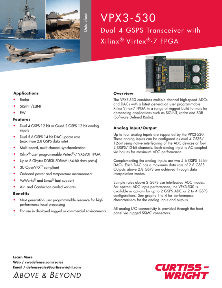
Data Sheet
VPX3-530
D u a l 4 GS PS Tr a n s c e i v e r w ith
X i l i n x ® V i r t e x ®- 7 F PGA
Applications
Overview
Radar
SIGINT/ELINT
EW
The VPX3-530 combines multiple channel high-speed ADCs
and DACs with a latest generation user programmable
Xilinx Virtex-7 FPGA in a range of rugged build formats for
demanding applications such as SIGINT, radar and SDR
(Software Defined Radio).
Features
Dual 4 GSPS 12-bit or Quad 2 GSPS 12-bit analog
inputs
Dual 5.6 GSPS 14-bit DAC update rate
(maximum 2.8 GSPS data rate)
Multi-board, multi-channel synchronization
Xilinx® user programmable Virtex®-7 VX690T FPGA
Up to 8 Gbytes DDR3L SDRAM (64-bit data paths)
3U OpenVPX™ compliant
Onboard power and temperature measurement
VxWorks® and Linux® host support
Air- and Conduction-cooled variants
Benefits
Next generation user programmable resource for high
performance local processing
For use in deployed rugged or commercial environments
Learn More
Web / cwcdefense.com/sales
Email / defensesales@curtisswright.com
Analog Input/Output
Up to four analog inputs are supported by the VPX3-530.
These analog inputs can be configured as dual 4 GSPS/
12-bit using native interleaving of the ADC devices or four
2 GSPS/12-bit channels. Each analog input is AC coupled
via baluns for maximum ADC performance.
Complementing the analog inputs are two 5.6 GSPS 14-bit
DACs. Each DAC has a maximum data rate of 2.8 GSPS.
Outputs above 2.8 GSPS are achieved through data
interpolation modes.
Sample rates above 2 GSPS use interleaved ADC modes.
For optimal ADC input performance, the VPX3-530 is
available in options for up to 2 GSPS ADC or 2 to 4 GSPS
configurations. See graphs 1 to 4 for performance
characteristics for the analog input and outputs.
All analog I/O connectivity is provided through the front
panel via rugged SSMC connectors.
SNR
ADC I0
55.00
P
40.00
35.00
ADC0I
ADC1Q
ADC I1
ADC1I
y
r
a
y
r
a
55.00
n
i
m
50.00
SINAD [dBc]
li
e
r
45.00
li
e
r
45.00
P
40.00
30.00
35.00
0.00
500.00
1000.00
1500.00
2000.00
2500.00
3000.00
0.00
500.00
1000.00
1500.00
Data Frequency [MHz]
SFDR
0
ADC1I
65.00
SFDR dBc
-80
-100
1000.00
1000
P
1200
1400
y
r
a
n
i
m
-90
30.00
500.00
800
li
e
r
-60
-70
35.00
0.00
600
-50
Pr
40.00
400
-40
in
m
i
l
e
200
-30
y
ar
60.00
DAC1
-20
ADC1Q
45.00
3000.00
DAC0
SFDR (Baseband)
ADC I0
50.00
2500.00
Figure 4: ADC SINAD (non-DES mode)
ADC Q0
70.00
55.00
2000.00
Data Frequency [MHz]
Figure 1: ADC SNR (non-DES mode)
SFDR [dBc]
ADC0Q
60.00
ADC Q1
n
i
m
50.00
SNR [dBc]
SINAD
ADC Q0
60.00
1500.00
2000.00
2500.00
Frequency MHz
3000.00
Data Frequency [MHz]
Figure 5: DAC SFDR
Figure 2: ADC SFDR (non-DES mode)
ENOB
ADC Q0
ADC I1
9.00
ADC Q1
ADC I1
8.50
r
a
in
8.00
ENOB [bitC]
7.50
y
m
i
l
e
7.00
Pr
6.50
6.00
5.50
5.00
0.00
500.00
1000.00
1500.00
2000.00
2500.00
3000.00
Data Frequency [MHz]
Figure 3: ADC ENOB (non-DES mode)
2
Curtiss-Wright Defense Solutions / cwcdefense.com
Sample Clocks, Triggers and Synchronization
The VPX3-530 does not use a local sample clock, but
instead an external source for maximum performance.
The VPX3-530 provides the choice of two RF sample clock
sources through the front panel. Modes are supported
that allow synchronous ADC and DAC data sampling or
independent sample clock for the ADCs and DACs. This
allows coherent input and output sampling or the ability to
operate the ADCs and DACs separately.
Trigger inputs and outputs are provided through front panel
connectors, though with suitable HDL, backplane based
triggers are also possible.
Both 'Trigger In' and 'Trigger Out' are single-ended LVPECL
buffered signals connected to the host FPGA. These signals
are also used as part of the mechanism to synchronize the
ADCs on multiple VPX3-530 cards; effectively the function
of these signals is changed to a sync mode when this is
required.
The ADC12D2000RF ADCs support multiple modes, but
can be separated into interleaved and non-interleaved
modes for the two ADCs in each device. In the noninterleaved mode, each ADC is synchronously clocked off
the same sample clock edge. For the interleaved mode,
Dual Edge Sampling (DES) is used in which one ADC is
clocked off rising edge of the sample clock and the other
ADC is clocked off the falling edge of the sample clock. The
standard build configurations of the VPX3-530 use two dual
ADC devices. Since the ADC devices can operate up to
2 GSPS per channel in non-interleaved mode or up to
4 GSPS in DES interleaved mode, the maximum sample
clock input frequency is 2GHz.
Additional signals are unbuffered 1.8V LVDS or RS-485
via the VPX P2 connector. These are available for the user
application. A 1PPS signal input is also provided through
the VPX P0 connector (user HDL required to implement).
Xilinx Virtex-7 FPGA
The VPX3-530 is built around a user programmable Xilinx
Virtex-7 VX690T FPGA resource (speed grade 2). Virtex-7
is a member of Xilinx's 28nm 7-Series family. The FPGA is
supported by high speed DDR3L memory resources directly
connected the FPGA.
The VPX3-530’s AD9129 DACs support two general
modes; direct baseband update and mixed mode. The
direct mode allows data updates of up to 2.8 GSPS with
a corresponding output rate and using up to a 2.8GHz
sample clock. Mix mode allows a doubling of DAC output
rates of up to 5.6 GSPS though interpolation of the input
data and sample clock. It should be noted that the minimum
DAC sample clock is 1.4GHz.
The FPGA configuration images can be stored in either
the flash memory or DDR SDRAM configuration memory
and can be updated by the host CPU using the PCI
Express® (PCIe) interface. The DDR SDRAM resource allows
configurations to be downloaded from the host and bypass
the non-volatile flash. Since SDRAM based configuration
is volatile, it is an attractive mode for security sensitive
applications and allows the VPX3-530 to be more easily
declassified should the need arise.
Since the clocking modes supported by the ADC and DAC
devices, there is a use case where using clocks above
2GHz would require the ADCs to operate in DES mode,
while the DAC operate in single edge clock up to 2.8GHz
i.e. the ADCs will sample at twice the rate that the DAC
updates. If this is an issue, the DAC could be programmed
to operate in mix mode, thereby ensure common input and
out update rates. See diagram below for an overview of the
input clock structure.
ADC 0
ADC 1
I
ADC
Q
>
ADC
Q
ADC
RF CLK 0
DAC 0
>
÷4 clock
divider
x4 demux
ADC
I
Fanout
Buffer
The FPGA can be reconfigured from any one of a number
of images indexed in the flash including a write protected
recovery configuration. FPGA configuration from either
flash or DDR SDRAM can also take advantage of AES
encryption.
Multiple Memory Banks
x4 demux
÷4 Sample clock
The VPX3-530 supports two banks of 256 M x 64-bit or
512 M x 64-bit DDR3L SDRAM, each directly connected
to the FPGA. As each memory bank is independently
connected to the FPGA, there is great flexibility in how they
may be used. Each memory bank supports read or write
bandwidths of around 9.6 Gbytes/sec.
FPGA
> DAC
RF CLK 1
Switch
> DAC
DAC 0
Figure 6: Overview of RF Sample Clock Inputs
3
Curtiss-Wright Defense Solutions / cwcdefense.com
Power and Temperature Measurement
FusionXF Software/HDL Support
The VPX3-530 includes built in power (including current
and temperature) measurement capabilities. For rugged
applications using high power components like FPGAs, this
provides critical feedback on the health of the card and
whether recalibration might be recommended.
Curtiss-Wright’s FusionXF Development Kit includes software,
HDL and utilities complete with examples for using the
VPX3-530. FusionXF includes a C programming language
API, driver framework and sophisticated DMA support. One
of the core elements to the FusionXF development kit is a
framework for adding in new IP functionality or capabilities
to the FPGA easily and effectively.
Elapsed Time Indicator
The VPX3-530 incorporates an Elapsed Time Indicator (ETI).
This provides the ability to determine the total accumulated
time (up to 34 years) the card has been under power and
to support system maintenance plans.
Software utilities are provided for configuring the FPGA.
These include flash programming and configuring the FPGA
from one of many indexed images in flash.
FusionXF supports VxWorks and Linux Fedora operating
systems. Additional operating systems, such as Windows, or
other distributions of Linux can be considered on request.
JTAG
A standard 2mm JTAG header is provided on the VPX3530. This allows a standard Xilinx JTAG pod to be used for
debug.
Rugged Build Options
A range of environmental requirements are addressed by
the VPX3-530 including commercial, air-cooled rugged and
conduction-cooled. Contact Curtiss-Wright for details.
VPX Connectivity
The VPX3-530 supports OpenVPX profiles for PCI Express®
(PCIe) Generation 1 and 2. Contact factory for PCIe Gen 3
support.
PCIe is supported through direct connectivity to the Xilinx
Virtex-7 FPGA which enables up to x8 lane width over the
VPX P1 connector. In addition, a second bank of x8 HSS
links, again directly connected to the FPGA is provided over
the VPX P1 connector. This bank of x8 HSS links is fully
user programmable with each link able to operate over 10
Gbps. This is ideal for efficient inter-FPGA communications
or to implement I/O ports such as Serial FPDP or 10/40
GbE. Note: the use of Serial FPDP or Ethernet protocols
requires additional HDL. The x8 PCIe port can also be user
defined as the backplane links are directly connected to the
FPGA without the use of bridges.
Figure 7: Air and Conduction-cooled VPX3-530 variants
VPX P2 connectivity is reserved for the "parallel" I/O ports
from the FPGA and configured as differential I/O pairs.
Two of the input I/O pairs is buffered using RS-485/422
compliant devices to the FPGA, two further FPGA driven
RS-485/422 pairs are outputs to the backplane. The
remaining 28 differential VPX P2 I/O are connected
directly to the FPGA and can be defined as either inputs or
outputs as the application requires.
The VPX3-530 requires +5V and 3V3_Aux power supplies
thereby allowing greater system flexibility. +12V and 3V3
power inputs are not required.
4
Curtiss-Wright Defense Solutions / cwcdefense.com
JTAG
Header
1PPS
JTAG
5V/3V3
Clock
distribution/
control
Balun
Balun
Balun
IO Sub-system
ADC/DAC clocks
4GSPS 12b
(2x 2.0 GSPS)
5.6 GSPS
14b DAC
4GSPS 12b
(2x 2.0 GSPS)
Balun
5.6 GSPS
14b DAC
Balun
Balun
LVPECL
LVPECL
IO Sub-system
ADC/DAC clocks
4GSPS 12b
(2x 2.0 GSPS)
FPGA Sub-system
FLASH SDRAM
Configuration
Controller
1PPS
5V/3V3
2x RS485
2x RS485
x28 LVDS (1.8V) I/O
x8 GTH/HSS
x8 HSS/PCIe 2/3
JTAG
Temperature
Sensors
JTAG
Header
Power
Sensors
Elapsed Time
Indicator
x64
2x RS485
2x RS485
x28 LVDS (1.8V) I/O
x8 GTH/HSS
x8 HSS/PCIe 2/3
JTAG
1PPS
5V/3V3
JTAG
Header
Temperature
Sensors
Elapsed Time
Indicator
Power
Sensors
2/4GB DDR3
SDRAM
Virtex-7
VX690T
FPGA
x64
2/4GB DDR3
SDRAM
FPGA Sub-system
FLASH SDRAM
Configuration
Controller
x64
1PPS
5V/3V3
JTAG
Power
Sensors
Temperature
Sensors
2/4GB DDR3
SDRAM
Virtex-7
VX690T
FPGA
x64
2/4GB DDR3
SDRAM
Configuration
Controller
FLASH SDRAM
FPGA Sub-system
JTAG
Header
x8 HSS/PCIe 2/3
x8 GTH/HSS
2x RS485
2x RS485
x28 LVDS (1.8V) I/O
4xPCIe2
Power
Sensors
Temperature
Sensors
Elapsed Time
Indicator
Clock
distribution/
control
Balun
Balun
Balun
IO Sub-system
Elapsed Time
Indicator
x64
4xPCIe2
4xPCIe2
4xPCIe2
FLASH SDRAM
FPGA Sub-system
Configuration
Controller
x8 HSS/PCIe 2/3
x8 GTH/HSS
x28 LVDS (1.8V) I/O
2x RS485
2x RS485
4GSPS 12b
(2x 2.0 GSPS)
5.6 GSPS
14b DAC
Balun
Balun
5.6 GSPS
14b DAC
4GSPS 12b
(2x 2.0 GSPS)
ADC/DAC clocks
Balun
LVPECL
LVPECL
Clock
distribution/
control
Balun
Balun
Balun
4GSPS 12b
(2x 2.0 GSPS)
Virtex-7
VX690T
FPGA
Clock
distribution/
control
Balun
Balun
Balun
Balun
Balun
Balun
LVPECL
LVPECL
5.6 GSPS
14b DAC
4GSPS 12b
(2x 2.0 GSPS)
4GSPS 12b
(2x 2.0 GSPS)
IO Sub-system
ADC/DAC clocks
DDR3/
GDDR5
5.6 GSPS
14b DAC
PCIe
FPGA Sub-system
FLASH SDRAM
Configuration
Controller
1PPS
5V/3V3
2x RS485
2x RS485
x28 LVDS (1.8V) I/O
x8 GTH/HSS
x8 HSS/PCIe 2/3
JTAG
Temperature
Sensors
JTAG
Header
Power
Sensors
Elapsed Time
Indicator
x64
2/4GB DDR3
SDRAM
Virtex-7
VX690T
FPGA
x64
2/4GB DDR3
SDRAM
4xPCIe2
IO Sub-system
ADC/DAC clocks
4GSPS 12b
(2x 2.0 GSPS)
x64
5V/3V3
x8 HSS/PCIe 2/3
JTAG
Temperature
Sensors
JTAG
Header
1PPS
Elapsed Time
Indicator
Power
Sensors
2/4GB DDR3
SDRAM
Virtex-7
VX690T
FPGA
x64
2/4GB DDR3
SDRAM
FPGA Sub-system
FLASH SDRAM
Configuration
Controller
x8 GTH/HSS
Dual 4GSPS (Quad 2GSPS)
Dual 4GSPS (Quad 2GSPS)
Clock
distribution/
control
Balun
Balun
Balun
5.6 GSPS
14b DAC
4GSPS 12b
(2x 2.0 GSPS)
Balun
5.6 GSPS
14b DAC
Balun
Balun
LVPECL
IO Sub-system
ADC/DAC clocks
4GSPS 12b
(2x 2.0 GSPS)
4GSPS 12b
(2x 2.0 GSPS)
x28 LVDS (1.8V) I/O
Balun
5.6 GSPS
14b DAC
8 xPCIe 2
MXM 3.0 type A/B
XMC
x4 HSS link
x4 HSS link
x4 PCIe link
LVPECL
Clock
distribution/
control
Balun
Balun
Balun
Balun
Virtex-7
VX690T
FPGA
2x RS485
2x RS485
Balun
x4 PCIe link
Direct DMA from FPGA to GPGPU
x4 PCIe link
Curtiss-Wright Defense Solutions / cwcdefense.com
5
x64
8 xPCIe 2
Quad Receiver
Quad Receiver
Quad Receiver
Video
8 xPCIe 2
x64
2/4GB DDR3
SDRAM
1333 MHz
5.6 GSPS
14b DAC
8 xPCIe 2
PCIe x16
1333 MHz
DDR3
SDRAM
2-8 GB
Intel® Core™ i7
Quad Core
2.1 GHz
DDR3
SDRAM
2-8 GB
x64
Transceiver inputs
Figure 10: Integration with a GPGPU
with Direct DMA Support (via PCIe
Bridge)
2/4GB DDR3
SDRAM
8 xPCIe 2
5.6 GSPS
14b DAC
XMC
XCLK1
Balun
XMC
5.6 GSPS
14b DAC
8 xPCIe 2
Balun
24xPCIe2
Switch
w/ DMA
I/O
LVPECL
LVPECL
1333MHz
2/4GB DDR3
SDRAM
DDR3
SDRAM
2-8 GB
Intel Core™ i7
Quad Core
2.1 GHz
1333MHz
2/4GB DDR3
SDRAM
®
DDR3
SDRAM
2-8 GB
24xPCIe2
Switch
w/ DMA
I/O
24xPCIe2
Switch
w/ DMA
I/O
Dual 4GSPS
Transceiver IO
Dual 4GSPS
Transceiver IO
Figure 8: Quad Transceiver Example
Balun
1333 MHz
LVPECL
LVPECL
DDR3
SDRAM
2-8 GB
Dual 4GSPS (Quad 2GSPS)
Clocks & sync
SBC + Master
Clock Generator
Figure 9: SIGINT/Direction Finding
Example
1333 MHz
Intel® Core™ i7
Quad Core
2.1 GHz
DDR3
SDRAM
2-8 GB
4xPCIe2
Example Configurations
x4 PCIe link
x4 PCIe link
Table 1: VPX3-530 VPX Pinout
Pin
VPX P0
G
D
C
B
A
NC
NC
NC
NC
NC
NC
2
NC
NC
NC
NC
NC
NC
NC
3
5V
5V
5V
NC
5V
5V
5V
4
IPMBB_SCL
IMPBB_SDA
GND
NC
GND
SYSRST
NVMRO
5
GAP
GA4
GND
3V3_AUX
GND
IPMBA_SCL
IPMBA_SDA
6
GA3
GA2
GND
NC
GND
GA1
GA0
7
JTAG_TCK
GND
JTAG_TD0
JTAG_TDI
GND
JTAG_TMS
JTAG_TRST
8
GND
REF_CLK_N
REF_CLK_P
GND
1PPS_N
1PPS_P
GND
G
F
E
D
C
B
A
1
MBSC_SYNC
GND
PCIE_TX_0_P
PCIE_TX_0_N
GND
PCIE_RX_0_P
PCIE_RX_0_N
2
GND
PCIE_TX_1_P
PCIE_TX_1_N
GND
PCIE_RX_1_P
PCIE_RX_1_N
GND
3
V_BAT
GND
PCIE_TX_2_P
PCIE_TX_2_N
GND
PCIE_RX_2_P
PCIE_RX_2_N
4
GND
PCIE_TX_3_P
PCIE_TX_3_N
GND
PCIE_RX_3_P
PCIE_RX_3_N
GND
5
SYSCOON_L
GND
PCIE_TX_4_P
PCIE_TX_4_N
GND
PCIE_RX_4_P
PCIE_RX_4_N
6
GND
PCIE_TX_5_P
PCIE_TX_5_N
GND
PCIE_RX_5_P
PCIE_RX_5_N
GND
7
P1_SE3
GND
PCIE_TX_6_P
PCIE_TX_6_N
GND
PCIE_RX_6_P
PCIE_RX_6_N
8
GND
PCIE_TX_7_P
PCIE_TX_7_N
GND
PCIE_RX_7_P
PCIE_RX_7_N
GND
9
P1_SE4
GND
HSS_TX_0_P
HSS_TX_0_N
GND
HSS_RX_0_P
HSS_RX_0_N
10
GND
HSS_TX_1_P
HSS_TX_1_N
GND
HSS_RX_1_P
HSS_RX_1_N
GND
11
P1_SE5
GND
HSS_TX_2_P
HSS_TX_2_N
GND
HSS_RX_2_P
HSS_RX_2_N
12
GND
HSS_TX_3_P
HSS_TX_3_N
GND
HSS_RX_3_P
HSS_RX_3_N
GND
13
P1_SE6
GND
HSS_TX_4_P
HSS_TX_4_N
GND
HSS_RX_4_P
HSS_RX_4_N
14
GND
HSS_TX_5_P
HSS_TX_5_N
GND
HSS_RX_5_P
HSS_RX_5_N
GND
15
P1_SE7
GND
HSS_TX_6_P
HSS_TX_6_N
GND
HSS_RX_6_P
HSS_RX_6_N
16
GND
HSS_TX_7_P
HSS_TX_7_N
GND
HSS_RX_7_P
HSS_RX_7_N
GND
1
P2_SE0
GND
LVDS_1_N
LVDS_1_P
GND
LVDS_0_N
LVDS_0_P
2
GND
LVDS_3_N
LVDS_3_P
GND
LVDS_2_N
LVDS_2_P
GND
LVDS_5_P1
Pin
VPX P2
E
NC
Pin
VPX P1
F
1
G
F
E
D
C
B
A
3
P2_SE1
GND
LVDS_5_N1
GND
LVDS_4_N
LVDS_4_P
4
GND
LVDS_7_N
LVDS_7_P
GND
LVDS_6_N
LVDS_6_P
GND
5
P2_SE2
GND
LVDS_9_N
LVDS_9_P
GND
LVDS_8_N
LVDS_8_P
6
GND
LVDS_11_N
LVDS_11_P
GND
LVDS_10_N
LVDS_10_P
GND
7
P2_SE3
GND
LVDS_13_N
LVDS_13_P
GND
LVDS_12_N
LVDS_12_P
8
GND
LVDS_15_N
LVDS_15_P
GND
LVDS_14_N
LVDS_14_P
GND
9
P2_SE4
GND
LVDS_17_N
LVDS_17_P
GND
LVDS_16_N
LVDS_16_P
10
GND
LVDS_19_N
LVDS_19_P
GND
LVDS_18_N
LVDS_18_P
GND
11
P2_SE5
GND
LVDS_21_N
LVDS_21_P
GND
LVDS_20_N
LVDS_20_P
12
GND
LVDS_23_N2
LVDS_23_P2
GND
LVDS_22_N1
LVDS_22_P1
GND
13
P2_SE6
GND
LVDS_25_N2
LVDS_25_P2
GND
LVDS_24_N2
LVDS_24_P2
LVDS_26_P1
GND
14
GND
LVDS_27_N
LVDS_27_P
GND
LVDS_26_N1
15
P2_SE7
GND
RS485_in0_N
RS485_in0_P
GND
RS485_out0_N
RS485_out0_P
16
GND
RS485_in1_N
RS485_in1_P
GND
RS485_out1_N
RS485_out1_P
GND
Note 1: Multi-Region Clock Capable (MRCC)
Note 2: Single-Region Clock Capable (SRCC)
6
Curtiss-Wright Defense Solutions / cwcdefense.com
Table 2: Specifications
FPGA
VPX
Device
Xilinx Virtex-7 VX690T (speed grade 2)
(contact factory for alternative FPGA sizes)
Configuration
Over PCIe interface
1 Gbit flash (FPGA boot/configuration including
recovery image)
512 Mbit SDRAM (FPGA volatile configuration)
JTAG/ChipScope Pro port
OpenVPX Profiles
MOD3-PAY-1D-16.2.6-2 and
MOD3-PER-1F-16.3.2-2
VPX P0
VPX P1
x8 HSS (user defined up to 10.1 Gbps per lane,
PCIe 1 or PCIe 2 (contact factory for PCIe Gen 3)
x8 HSS (user defined up to 10.1 Gbps per lane)
VPX P2
x2 RS-422/485 inputs (FPGA controlled)
x2 RS-422/485 outputs (FPGA controlled)
x28 1.8V LVDS (FPGA controlled)
Board Pitch
Conduction-cooled: 0.85"
Air-cooled: 1"
Analog Input (contact factory for alternative sample rates and performance)
Number of Channels
2 (4 GSPS) or 4 (2 GSPS)
no ADCs fitted (build option)
Sampling Frequency
Up to 4 GSPS per channel
Full Scale Input
Voltage
Up to 4 dBm adjustable
Analog Bandwidth
1.5 GHz @ 2 GSPS
SFDR (typ)
61 dBc @ 498 MHz (2 GSPS)
SNR (typ)
54 dBc @ 498 MHz (2 GSPS)
ENOB (typ)
8.5 bits @ 498 MHz (2 GSPS)
Input Impedance
50 Ohm, AC coupled
Input Connector
Front panel SSMC
Memory
Analog Output
Type
DDR3L SDRAM
Capacity
Total: 4 or 8 Gbytes
2x 256 M x 64-bit or
2x 512 M x 64-bit
Bandwidth
>9.6 Gbytes/sec (read or write) per bank
Number of Channels 2 or no DACs fitted (build option)
Sampling Frequency
Up to 5.6 GSPS update rate
Up to 2.8 GSPS direct RF synthesis
Full Scale Output
-3 dBm (contact factory for other input ranges)
SFDR (typ)
-68 dBc
IMD (typ)
-83 dBc
Software/HDL
Support/Utilities
FusionXF development kit
FPGA/flash programming, diagnostics
Host Drivers
VxWorks or Linux (Fedora)
(contact factory for Windows support)
HDL example
Memory interfaces, PCIe, data DMA, data
acquisition, data playback
Clock Input
Clock Input Sources
Mode 1: RF Clock 0 to all ADC and DACs
(RF Clock 1 not used)
Mode 2: RF Clock 0 to ADCs, RF Clock 1 to
DACs
Clock Input
50 Ohm, AC coupled LVPECL
Miscellaneous
Single-ended, 50 Ohm, LVPECL buffered to host
Trigger Input/Output
FPGA
Clock Input
Connector
5V: 19.8A (max)
3V3_Aux: 0.8A (max)
3V3: not required
VBAT: 3V (nom)
12V: not required
1PPS
REF_CLK
JTAG
LED
2, user controlled via FPGA
Elapsed Time
Indicator (ETI)
0.25 second resolution, maximum accumulated time
34 years
Power
Card input voltage and current measurement facility
Front panel SSMC
Table 3: Ordering Information
DAC
Memory
VPX3-530- A061240
4x 2 GSPS
ADC
2x 5.6 GSPS (2.8 GSPS update rate)
2x 4Gbytes
AC L0
Optimized for up 2 GSPS mode
VPX3-530- A161240
4x 2 GSPS
2x 5.6 GSPS (2.8 GSPS update rate)
2x 4Gbytes
AC L100
Optimized for up 2 GSPS mode
VPX3-530- C261240
4x 2 GSPS
2x 5.6 GSPS (2.8 GSPS update rate)
2x 4Gbytes
CC L200
Optimized for up 2 GSPS mode
VPX3-530- A062240
2x 4 GSPS
2x 5.6 GSPS (2.8 GSPS update rate)
2x 4Gbytes
AC L0
Optimized for up 4 GSPS mode
VPX3-530- A162240
2x 4 GSPS
2x 5.6 GSPS (2.8 GSPS update rate)
2x 4Gbytes
AC L100
Optimized for up 4 GSPS mode
VPX3-530- C262240
2x 4 GSPS
2x 5.6 GSPS (2.8 GSPS update rate)
2x 4Gbytes
CC L200
Optimized for up 4 GSPS mode
7
Environmental Level
Comment
Curtiss-Wright Defense Solutions / cwcdefense.com
RF CLK 0
RF CLK 1
I/O Sub-system FPGA Sub-system
Clock
Distribution/
Control
ADC/DAC clocks
ADC 0
Balun
ADC 1
Balun
ADC 2
Balun
ADC 3
Balun
DAC 0
Balun
5.6 GSPS
14b DAC
DAC 1
Balun
5.6 GSPS
14b DAC
TRIG Out
TRIG In
Flash-
SDRAM
Configuration
Controller
4 GSPS 12b
(2x 2.0 GSPS)
Temperature
Sensors
5V/3V3
Power
Sensors
1PPS
Elapsed Time
Indicator
JTAG
JTAG
Header
x8 HSS/PCIe 2/3
4 GSPS 12b
(2x 2.0 GSPS)
x8 GTH/HSS
Virtex-7
VX690T
FPGA
x64
LVPECL
2/4 GB DDR3
SDRAM
LVPECL
x28 LVDS (1.8V) I/O
2x RS-485
2x RS-485
x64
2/4 GB DDR3
SDRAM
Figure 11: VPX3-530 Block Diagram
Warranty
The information in this document is subject to change
without notice and should not be construed as a
commitment by Curtiss-Wright Defense Solutions. While
reasonable precautions have been taken, Curtiss-Wright
assumes no responsibility for any errors that may appear
in this document. All products shown or mentioned are
trademarks or registered trademarks of their respective
owners.
This product has a one year warranty.
Contact Information
To find your appropriate sales representative:
© Copyright 2013, Curtiss-Wright
All Rights Reserved. MKT-DS-VPX3-530-26Mar2014v4
Website: www.cwcdefense.com/sales
Email: defensesales@curtisswright.com
Technical Support
For technical support:
Website: www.cwcdefense.com/support
Email: support@curtisswright.com
8
Curtiss-Wright Defense Solutions / cwcdefense.com


