Product Preview
MICROSEMI CLOCK SYNTHESIS PRODUCTS
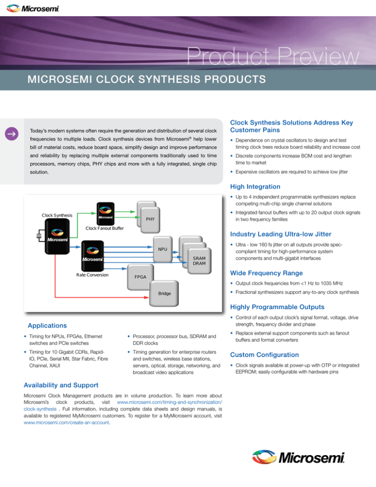
Today’s modern systems often require the generation and distribution of several clock
frequencies to multiple loads. Clock synthesis devices from Microsemi® help lower
bill of material costs, reduce board space, simplify design and improve performance
and reliability by replacing multiple external components traditionally used to time
Clock Synthesis Solutions Address Key
Customer Pains
• Dependence on crystal oscillators to design and test
timing clock trees reduce board reliability and increase cost
processors, memory chips, PHY chips and more with a fully integrated, single chip
• Discrete components increase BOM cost and lengthen
time to market
solution.
• Expensive oscillators are required to achieve low jitter
High Integration
• Up to 4 independent programmable synthesizers replace
competing multi-chip single channel solutions
Clock Synthesis
• Integrated fanout buffers with up to 20 output clock signals
in two frequency families
PHY
Clock Fanout Buffer
Industry Leading Ultra-low Jitter
NPU
SRAM
DRAM
Rate Conversion
• Ultra - low 160 fs jitter on all outputs provide speccompliant timing for high-performance system
components and multi-gigabit interfaces
Wide Frequency Range
FPGA
• Output clock frequencies from <1 Hz to 1035 MHz
Bridge
• Fractional synthesizers support any-to-any clock synthesis
Highly Programmable Outputs
• Control of each output clock’s signal format, voltage, drive
strength, frequency divider and phase
Applications
• Timing for NPUs, FPGAs, Ethernet
switches and PCIe switches
• Processor, processor bus, SDRAM and
DDR clocks
• Timing for 10 Gigabit CDRs, RapidIO, PCIe, Serial MII, Star Fabric, Fibre
Channel, XAUI
• Timing generation for enterprise routers
and switches, wireless base stations,
servers, optical, storage, networking, and
broadcast video applications
Availability and Support
Microsemi Clock Management products are in volume production. To learn more about
Microsemi’s clock products, visit www.microsemi.com/timing-and-synchronization/
clock-synthesis . Full information, including complete data sheets and design manuals, is
available to registered MyMicrosemi customers. To register for a MyMicrosemi account, visit
www.microsemi.com/create-an-account.
• Replace external support components such as fanout
buffers and format converters
Custom Configuration
• Clock signals available at power-up with OTP or integrated
EEPROM; easily configurable with hardware pins
Microsemi Clock Synthesis Products
Featured Products
ZL30250 and ZL30251
• Industry leading low jitter provides spec-compliant timing for
multi-gigabit interfaces
ZL30251
ic1_p/n
DIV
DIV
oc1_p/n
DIV
DIV
oc2_p/n
DIV
oc3_p/n
ic2_p/n
APLL
ic3/gpio3
xout
xin
Crystal
Driver
DIV
x2
EEPROM
o Any-to-any frequency synthesis / conversion generates any
clock rate from <1Hz to 1035 MHz with jitter as low as 160 fs
• Spread-spectrum
o +/- 0.5% meets low EMI specifications
• Accurate numerically controlled oscillator
2
Configuration
and Status
SPI/I C
Slave
o Replaces expensive high end analog VCXOs
GPIO/
Alarms
• Pin-selectable custom configuration
Control
Interface
o Easy implementation; up to 4 configurations
• Small 5mm x 5mm QFN
GPIO
MAX24405/10 and MAX24505/10
MAX24510
ic1_p/n
ic2_p/n
mclk_p/n
xout
xin
APLL1
Crystal
Driver
APLL2
DIV
oc1_p/n
DIV
oc2_p/n
DIV
oc3_p/n
DIV
oc4_p/n
DIV
oc5_p/n
DIV
oc6_p/n
DIV
oc7_p/n
DIV
oc8_p/n
DIV
oc9_p/n
DIV
oc10_p/n
• Ultra-low jitter output clocks provide spec-compliant timing for
multi-gigabit interfaces
o Any-to-any frequency synthesis / conversion from 10 MHz to
750 MHz with ultra – low 180 fs RMS jitter
• On-chip fanout buffers with flexible output configuration
o Up to 20 output clock signals in two frequency families
o Control over each output clock’s signal format, voltage
and drive strength
o Frequency divider and phase adjustment per output
EEPROM
Configuration
and Status
Control
Interface
SPI/I2C
Slave
JTAG
GPIO
JTAG
• 10mm x 10mm CSBGA
ZL30230, ZL30236 and ZL30237
ZL30230
Clock Generation 0
Precision
Synthesizer 0
Clock Generation 1
Precision
Synthesizer 1
Master
Clock
Clock Generation 2
General
Synthesizer 2
Clock Generation 3
General
Synthesizer 3
Configuration
and status
SPI/I 2C
Slave
JTAG
Control
Interface
JTAG
Microsemi Corporate Headquarters
One Enterprise, Aliso Viejo CA 92656 USA
Within the USA: +1(949) 380-6100
Sales: +1 (949) 380-6136
Fax: +1 (949) 215-4996
Email: sales.support@microsemi.com
hpdiff0_p/n
hpdiff1_p/n
hpdiff2_p/n
hpdiff3_p/n
hpoutclk0
hpoutclk1
hpdiff4_p/n
hpdiff5_p/n
hpdiff6_p/n
hpdiff7_p/n
hpoutclk2
hpoutclk3
out0
out1
out2
out3
• High channel integration with low output jitter replace competing
multi-chip solutions
o Up to 4 independent synthesizers generate any clock rate
from 1 kHz to 720 MHz with jitter below 0.7 ps RMS
• On-chip fanout buffers reduce component count and board cost
o 8 LVPECL outputs
o 8 outputs configurable as LVCMOS or LVDS/LVPECL/HCSL
• 11x11mm BGA
out4
out5
out6
out7
GPIO /
Alarms
GPIO
Microsemi Corporation (NASDAQ: MSCC) offers a comprehensive portfolio of semiconductor and system solutions
for communications, defense and security, aerospace and industrial markets. Products include high-performance and
radiation-hardened analog mixed-signal integrated circuits, FPGAs, SoCs and ASICs; power management products;
timing and synchronization devices and precise time solutions, setting the world’s standard for time; voice processing
devices; RF solutions; discrete components; security technologies and scalable anti-tamper products; Power-overEthernet ICs and midspans; as well as custom design capabilities and services. Microsemi is headquartered in Aliso
Viejo, Calif. and has approximately 3,400 employees globally. Learn more at www.microsemi.com.
© 2014 Microsemi Corporation. All rights reserved. Microsemi and the Microsemi logo are trademarks of Microsemi Corporation. All other trademarks and service
marks are the property of their respective owners.
Publication Number: MS7-006-13


