On chip power dissipation
advertisement

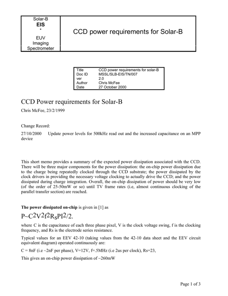
Solar-B EIS * CCD power requirements for Solar-B EUV Imaging Spectrometer Title Doc ID ver Author Date CCD power requirements for solar-B MSSL/SLB-EIS/TN/007 2.0 Chris McFee 27 October 2000 CCD Power requirements for Solar-B Chris McFee, 23/2/1999 Change Record: 27/10/2000 device Update power levels for 500kHz read out and the increased capacitance on an MPP This short memo provides a summary of the expected power dissipation associated with the CCD. There will be three major components for the power dissipation: the on-chip power dissipation due to the charge being repeatedly clocked through the CCD substrate; the power dissipated by the clock drivers in providing the necessary voltage clocking to actually drive the CCD; and the power dissipated during charge integration. Overall, the on-chip dissipation of power should be very low (of the order of 25-50mW or so) until TV frame rates (i.e, almost continuous clocking of the parallel transfer section) are reached. The power dissipated on-chip is given in [1] as P~C2V2f2RsPI2/2. where C is the capacitance of each three phase pixel, V is the clock voltage swing, f is the clocking frequency, and Rs is the electrode series resistance. Typical values for an EEV 42-10 (taking values from the 42-10 data sheet and the EEV circuit equivalent diagram) operated continuously are: C = 8nF (i.e ~2nF per phase), V=12V, f=.5MHz (i.e 2us per clock), Rs=23, This gives an on-chip power dissipation of ~260mW Page 1 of 3 Using representative values for the EEV-42 CCD series, and using representative clocking rates yields the following: CCD type 42-10 42-20 42-20 (MPP) 42-40 42-80 C (nF) 8 9 22 14 28 Rs (Ohms) 23 18 18 20 32 f=150khz 23mW 16mW 180mW 65mW 400mW f=330khz 113mW 112mW 674mW 303mW 1.9W f=500khz 261mW 260mW 1.5W 700mW 4.4W Total power dissipated by the clock drivers This is given (in both [1] and [2]) as P=fCV2 where C is the capacitance (3nF) and V is the clock pulse amplitude (12V) hence P= 576mW for a 42-10 clocked at 500khz. This is the maximum power dissipation that could be expected, i.e assuming 100% duty cycle. Typical power dissipations to be expected are CCD type 42-10 42-20 42-20 (MPP) 42-40 42-80 C (nF) 8 9 22 14 28 f=150khz 172mW 190mW 475mW 300mW 600mW f=330khz 380mW 427mW 1W 665mW 1.33W f=500khz 576mW 648mW 1.6W 1W 2W Quiescent power dissipation There will also be a quiescent power dissipation (given by VI) associated with the clock drivers during image integration. In total, there will be a number of clock drivers each contributing to the quiescent power dissipation. Two drivers are required for each parallel phase, one for each reset gate, one for each readout phase, and one for the dump gate (which will, however, usually have a lower duty cycle than the other drivers). The typical dc current drawn is around 7mA, this leads to a typical power dissipation as follows: parallel phases - 3x12x7 = 252 mW Left serial phases and reset - 2x11x7 = 154 mW Right serial phases and reset - 2x11x7 = 154 mW dump gate - 1x7 Vod = 30V = 77 mW Thus, the typical quiescent power dissipation is around 650 mW. In addition, the on-chip output node FET will also draw current. The output FET is shown below: 00 Vos 5-10k Page 2 of 3 For each output, (Vod-Vos)xI = 12 mW will be dissipated to the CCD and (Vos x I) = 168 mW is dissipated through the load resistor into the FPA. Power dissipated by the readout electronics The figures I have for the readout electronics come from Dave Walton and are "typical" figures for the Integral readout electronics, powered by desk top power supplies. During integration, the power dissipation of the ROE (including ADCs) is about 4 W, during clocking it is about 4.2 W. References [1] - CCD performance limitations: theory and practice. D J Burt [2] Charge coupled devices and their applications. J.D.E Beynon and D. R. Lamb Page 3 of 3


