AN681: Using the Si87xx Family of Digital Isolators
advertisement

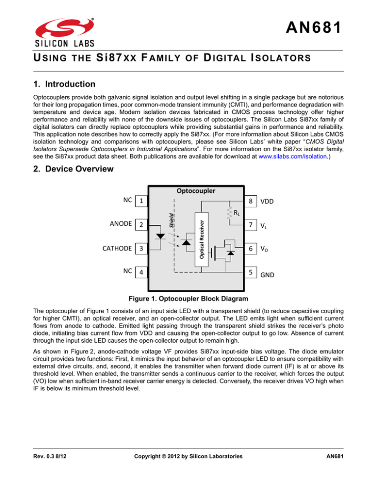
AN681 U SING T H E Si87 XX F AMILY O F D IGITA L I S O L A T O R S 1. Introduction Optocouplers provide both galvanic signal isolation and output level shifting in a single package but are notorious for their long propagation times, poor common-mode transient immunity (CMTI), and performance degradation with temperature and device age. Modern isolation devices fabricated in CMOS process technology offer higher performance and reliability with none of the downside issues of optocouplers. The Silicon Labs Si87xx family of digital isolators can directly replace optocouplers while providing substantial gains in performance and reliability. This application note describes how to correctly apply the Si87xx. (For more information about Silicon Labs CMOS isolation technology and comparisons with optocouplers, please see Silicon Labs’ white paper “CMOS Digital Isolators Supersede Optocouplers in Industrial Applications”. For more information on the Si87xx isolator family, see the Si87xx product data sheet. Both publications are available for download at www.silabs.com/isolation.) 2. Device Overview Optocoupler 1 2 CATHODE 3 NC 4 8 VDD 7 VL 6 VO 5 GND RL Optical Receiver ANODE Shield NC Figure 1. Optocoupler Block Diagram The optocoupler of Figure 1 consists of an input side LED with a transparent shield (to reduce capacitive coupling for higher CMTI), an optical receiver, and an open-collector output. The LED emits light when sufficient current flows from anode to cathode. Emitted light passing through the transparent shield strikes the receiver’s photo diode, initiating bias current flow from VDD and causing the open-collector output to go low. Absence of current through the input side LED causes the open-collector output to remain high. As shown in Figure 2, anode-cathode voltage VF provides Si87xx input-side bias voltage. The diode emulator circuit provides two functions: First, it mimics the input behavior of an optocoupler LED to ensure compatibility with external drive circuits, and, second, it enables the transmitter when forward diode current (IF) is at or above its threshold level. When enabled, the transmitter sends a continuous carrier to the receiver, which forces the output (VO) low when sufficient in-band receiver carrier energy is detected. Conversely, the receiver drives VO high when IF is below its minimum threshold level. Rev. 0.3 8/12 Copyright © 2012 by Silicon Laboratories AN681 AN681 Si87xx Isolator (SO‐8, DIP8, LGA8, SDIP6) VDD VDD1 VDD2 UVLO ANODE Diode ENABLE XMIT Emulator IF RECV ISOLATION GND1 ISOLATION VF Open Collector Output VO CATHODE GND GND2 INPUT DIE OUTPUT DIE Figure 2. Si87xx Isolator Block Diagram This simple but highly-effective Si87xx architecture offers substantial advantages over the optocoupler-based approach. Key differences between the Si87xx and conventional optocouplers include the following: 1. Fabricated in Mainstream Low-Power CMOS CMOS process technology enables high device integration and speed, low power consumption, high resistance to device temperature and aging effects, stable operation over the –40 to +125 C temperature range, and exceptionally high reliability. The Si87xx isolation barrier’s time-dependant device breakdown (TDDB) is 10 times lower, and its part-to-part matching is 14 times tighter than Gallium Arsenide-based (GaAs) optocouplers. 2. Use of a High-Frequency Carrier instead of Light The high-frequency carrier further enables low operating power, faster operation, and precise frequency discrimination for outstanding noise rejection. The fully differential signal path and high receiver selectivity provide CMTI immunity of >50 kV/µs (typ), external RF field immunity as high as 300 V/m, and magnetic field immunity above 1000 A/m for error-free operation. 3. Use of Proprietary Design Techniques to Suppress EMI Devices in this family meet FCC Part B emission standards using automotive J1750 (CISPR) test methods. For more information on CMOS isolator emissions, susceptibility, and reliability compared to optocouplers, please see Silicon Labs white paper “CMOS Isolators Supersede Optocouplers in Industrial Applications” available at www.silabs.com/isolation. 4. Use of Fully-Differential Architecture The single-ended optocoupler is vulnerable to disturbance or upset from common-mode voltage transients. In comparison, the Si87xx fully differential signal path architecture offers significantly higher CMTI compared to optocouplers. 2 Rev. 0.3 AN681 3. Device Application 3.1. Si87xx Device Transfer Characteristics The Si87xx is offered in three different grades, allowing the user to optimize input forward current versus CMTI. The Si87xx “A” grade and “C” grade have an optimum input diode current of 3 mA resulting in a minimum CMTI of 20 kV/µs(min), (35 kV/µs typical), while the “B” grade has an optimum input diode current of 6 mA resulting in a minimum CMTI of 35 kV/µs(min), (50 kV/µs typical). Referring to the “A” grade and “C” grade devices in Figure 3A, an open-collector output low event begins when the input current crosses the 1.2 mA current threshold, and input current must continue rising to 3.0 mA for the Si87xx to achieve rated CMTI performance. An open-collector output high event begins when the input current falls below the 1.1 mA threshold and must continue falling to zero for the Si87xx to achieve rated CMTI performance. The “B” grade device (Figure 3B) exhibits similar operation, with the exceptions of a low-going current threshold of 2.3 mA rising to 6 mA and a high-going input current turn-off threshold of 2.0 mA falling to zero. Note: All device grades must have a voltage drop of 1.7 to 2.8 V across the input during those periods where the open-collector output voltage is low. In addition, all device grades must operate at the optimum ON current to achieve rated performance. 20 mA Optimum On Current 6.0 mA 2.3 mA 0 mA 20 mA Minimum Current Required for Turn‐On (A and C Grade) Maximum Diode Emulator Input Current Output Low Maximum Diode Emulator Input Current Optimum On Current 3.0 mA 1.2 mA 1.1 mA 0 mA Output High Output Low 2.0 mA Output High Minimum Current Required for Turn‐On (B Grade) A B Figure 3. Device Transfer Characteristics Rev. 0.3 3 AN681 3.2. Replacing Optocouplers with Si87xx Optocouplers have external circuits for on/off LED control and current limiting. However, many applications add additional external circuitry to enhance performance, including circuits that reverse bias, overdrive, or short-circuit the LED to ensure that the correct state is maintained during a common-mode transient event. Other circuits include speed-up capacitors (low value capacitors placed across the LED current-limiting resistor as shown in Figure 4) to shorten propagation delay time. The Si87xx is compatible with these types of circuits; however most optocouplers draw higher input-side current than the Si87xx. As a result, retrofitting an optocoupler with the Si87xx often requires adjustment of the input-side series resistor R1 value. Ensure that the value of R1 is within the current limits shown in Figure 3. For more information on preferred input circuits, see the Si87xx data sheet available for download at www.silabs.com/isolation. Speed‐up Cap Optocoupler R1 Check the value of R1 to ensure it is within LED datasheet limits when retrofitting an optocoupler with the Si87xx Shorting iF Switch iR Forward (Overdrive) or Reverse Bias Figure 4. Optocoupler Supplemental Circuits 4 Rev. 0.3 Optocoupler LED AN681 3.3. Si87xx Input Circuit Configurations to Maximize CMT Performance The Si87xx can directly replace an optocoupler, provided the recommendations given in “3.2. Replacing Optocouplers with Si87xx” are adhered to. For best CMTI performance, the external input circuit should drive the Si87xx LED emulator with a low impedance source. The input circuit should not allow the LED emulator to be open-circuited (and therefore vulnerable to parasitic coupling that can corrupt data transmission) as shown in Figure 5. Control Si87xx ANODE R1 SW1 VIN Vulnerable to external parasitic coupling when S1 is off. CATHODE Figure 5. Poor Input Circuit Design The input circuit of Figure 6 is an example of a simple and effective input circuit. This circuit uses R2 to increase common-mode transient immunity (the lower the value of R2, the higher the CMTI). Resistor values of 100 for R1 and 1,000 for R2 are typical; however, these values can be adjusted to meet a designer’s needs as long as the Si87xx specifications are not violated. The user can optimize the value of R2 to achieve the best compromise between R2 power dissipation and CMTI performance. Moreover, R2 can be replaced with a switch to further enhance CMTI performance. Control Si87xx ANODE R1 SW1 VIN R2 CATHODE Figure 6. Cost-Effective High CMTI Immunity Circuit Rev. 0.3 5 AN681 The circuit of Figure 7 uses a complementary buffer (e.g., MCU port I/O pin, dedicated buffer, discrete circuit, etc.) to drive the ANODE pin. This circuit offers a balance of low impedance off/on drive and relatively low-power operation by optimizing the value of R1 for best CMTI performance. VDD Si87xx Control R1 ANODE Complementary output buffer (e.g. MCU port pin, driver, etc.) CATHODE Figure 7. Complementary Output Buffer Drive 6 Rev. 0.3 AN681 4. Layout Recommendations 4.1. Bypass Capacitors Output bypass capacitors consist of a parallel combination of a 0.1 μF high-frequency bypass and a 1 μF bulk capacitor connected between VDD and GND and placed as close as possible to the package. Ceramic capacitors should be used for VDD bypass because of their low impedance, high ripple current characteristics, small physical size, and cost effectiveness. 4.2. Layout Guidelines Ensure that no traces are routed through the creepage/clearance areas of the isolator. It is recommended that the NC pin on the Si87xx input side be connected to the input side ground plane; this increases CMTI performance by reducing coupling to the input pins. Minimize the trace lengths between isolators and connecting circuitry. To enhance the robustness of a design in excessively noisy systems, it is further recommended that the user also include 100 resistors in series with the outputs. 5. Summary The Si87xx is the ideal solution for upgrading optocouplers in existing and new designs. These isolators outperform their optocoupler-based counterparts and offer significant gains in device performance and reliability. Si87xx family members can directly replace any one of a number of optocouplers from various suppliers. Rev. 0.3 7 AN681 DOCUMENT CHANGE LIST Revision 0.1 to Revision 0.2 Updated "2. Device Overview" on page 1. Updated Figure 1 on page 1. Updated Figure 2 on page 2. Updated "3.1. Si87xx Device Transfer Characteristics" on page 3. Updated Figure 3 on page 3. Updatd "3.2. Replacing Optocouplers with Si87xx" on page 4. Updated Figure 4 on page 4. Updated Section 3.3 title on page 5. Updated "5. Summary" on page 7. Revision 0.2 to Revision 0.3 Updated "1. Introduction" on page 1. Updated "2. Device Overview" on page 1. Updated "3. Device Application" on page 3. 8 Rev. 0.3 AN681 NOTES: Rev. 0.3 9 Smart. Connected. Energy-Friendly Products Quality www.silabs.com/products www.silabs.com/quality Support and Community community.silabs.com Disclaimer Silicon Laboratories intends to provide customers with the latest, accurate, and in-depth documentation of all peripherals and modules available for system and software implementers using or intending to use the Silicon Laboratories products. Characterization data, available modules and peripherals, memory sizes and memory addresses refer to each specific device, and "Typical" parameters provided can and do vary in different applications. Application examples described herein are for illustrative purposes only. Silicon Laboratories reserves the right to make changes without further notice and limitation to product information, specifications, and descriptions herein, and does not give warranties as to the accuracy or completeness of the included information. Silicon Laboratories shall have no liability for the consequences of use of the information supplied herein. This document does not imply or express copyright licenses granted hereunder to design or fabricate any integrated circuits. The products must not be used within any Life Support System without the specific written consent of Silicon Laboratories. A "Life Support System" is any product or system intended to support or sustain life and/or health, which, if it fails, can be reasonably expected to result in significant personal injury or death. Silicon Laboratories products are generally not intended for military applications. Silicon Laboratories products shall under no circumstances be used in weapons of mass destruction including (but not limited to) nuclear, biological or chemical weapons, or missiles capable of delivering such weapons. Trademark Information Silicon Laboratories Inc., Silicon Laboratories, Silicon Labs, SiLabs and the Silicon Labs logo, CMEMS®, EFM, EFM32, EFR, Energy Micro, Energy Micro logo and combinations thereof, "the world’s most energy friendly microcontrollers", Ember®, EZLink®, EZMac®, EZRadio®, EZRadioPRO®, DSPLL®, ISOmodem ®, Precision32®, ProSLIC®, SiPHY®, USBXpress® and others are trademarks or registered trademarks of Silicon Laboratories Inc. ARM, CORTEX, Cortex-M3 and THUMB are trademarks or registered trademarks of ARM Holdings. Keil is a registered trademark of ARM Limited. All other products or brand names mentioned herein are trademarks of their respective holders. Silicon Laboratories Inc. 400 West Cesar Chavez Austin, TX 78701 USA http://www.silabs.com


