Lab 7 Operational Amplifiers and Negative Feedback Operational
advertisement
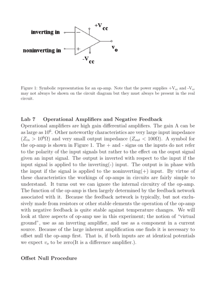
Figure 1: Symbolic representation for an op-amp. Note that the power supplies +Vcc and -Vcc may not always be shown on the circuit diagram but they must always be present in the real circuit. Lab 7 Operational Amplifiers and Negative Feedback Operational amplifiers are high gain differential amplifiers. The gain A can be as large as 106. Other noteworthy characteristics are very large input impedance (Zin > 106Ω) and very small output impedance (Zout < 100Ω). A symbol for the op-amp is shown in Figure 1. The + and - signs on the inputs do not refer to the polarity of the input signals but rather to the effect on the ouput signal given an input signal. The output is inverted with respect to the input if the input signal is applied to the inverting(-) input. The output is in phase with the input if the signal is applied to the noninverting(+) input. By virtue of these characteristics the workings of op-amps in circuits are fairly simple to understand. It turns out we can ignore the internal circuitry of the op-amp. The function of the op-amp is then largely determined by the feedback network associated with it. Because the feedback network is typically, but not exclusively made from resistors or other stable elements the operation of the op-amp with negative feedback is quite stable against temperature changes. We will look at three aspects of op-amp use in this experiment; the notion of “virtual ground”, use as an inverting amplifier, and use as a component in a current source. Because of the large inherent amplification one finds it is necessary to offset null the op-amp first. That is, if both inputs are at identical potentials we expect vo to be zero(It is a difference amplifier.). Offset Null Procedure Figure 2: Pinout for the 741 op-amp. Use Vcc = +- 12V from the fixed supplies. The pinout of the 741 is shown in Figure 2. Connect the circuit as shown in Figure 3. If you have a potentiometer on the experimenter’s board, adjust the pot until vo is approximately zero. You should be able to get within 5mV of ground. Virtual Ground Discussion The equivalent circuit for the op-amp is shown in Figure 4. Ri and Rc are the input resistances, which are both very large. The output impedance Ro is very small. The feedback netwrok is represented by β. It returns a portion of the output, βvo, to the input terminal. We wish to determine the difference v2 − v3. For Kirchoff’s loop going through the generator we obtain vo = a(v3 − v2) + io Ro (1) but v2 = βvo (2) βvo = βa(v3 − v2) + βio Ro v2 = βa(v3 − v2) + βio Ro (3) (4) Figure 3: Offset null procedure. Figure 4: Equivalent circuit for the op-amp. Ry (Ω) . . . Rw (Ω) . . . Vo (V) . . . V2 (V) . . . V3 (V) . . . V2 /V3 . . . Table 1: Op-amp golden rules (1 + aβ)v2 = aβv3 + βio Ro (5) we have β < 1 but still keep aβ >> 1 so aβ(v2 − v3) = βio Ro (6) or v2 − v3 = io Ro /a ≈ 0 (7) So it is a good approximation that the output adjusts in order that the feedback network makes v2 = v3. Circuit Build the circuit in Figure 5. Use the nominal values for the resistors. Check the relation v2 = v3 by filling in Table 1. Find the average ratio v2/v3 and the standard deviation. Notice if we set v3 = 0 by attaching terminal 3 to ground, for example, then v2 = 0 from the above results but no, or very little, current actually goes to ground through the op-amp because the input impedance is so high. This is the origin of the term virtual ground. Terminal 2 is at ground potential but no current goes to ground through the terminal 2 input. Inverting Amplifier Using the the approximation v2 = v3 we can easily compute the gain G of an op-amp with feedback. Consider Figure 6. Because v3 = v2 we also have v2 = 0. Also ia ≈ 0, hence ii + if = 0. Now vi = ii Ri and vo = if Rf and since G = vo /vi then G = if Rf /iiRi so G = −Rf /Ri . Build the circuit in Figure 6 and feed vi with a 100Ω/10KΩ voltage divider on the sine wave signal. Typical values for Figure 5: Circuit to check the effect of negative feedback on the relation between v2 and v3 . fnominal (Hz) . . T (S) . . tp (S) . . phase (rad) . . Vi (V) . . Vo (V) . . gain . . Table 2: Inverting Amplifier Rf are around 10KΩ and Ri around 1KΩ. Actually you can choose any set. For four frequencies covering the range of the signal generator measure the gain G and the phase shift between the input and output as in Table 2 Current Source A very good current source capable of sinking a current through a load to ground can be built with an op-amp. The simplest arrangement is in Figure 7. See Horowitz and Hill for other circuits. The circuit in Figure 7 can be understood as follows: (a) v3 is determined by the Rx /Ry voltage divider. (b) v3 = v2 = Ve . (c) Ie = (Vcc − Ve )/Re (d) Ie = Ic + Ib (e) Ic ≈ Ie for very small Ib (f) steps (e) and (d) work if Vce is bigger than the saturation voltage of a few tenths of a volt. Build the circuit in Figure 7. First calculate the approximate value of the maximum load resistor RLmax so that the transistor Vce is not saturated. Next choose five values of RL such that RL = RLmax , 2RLmax and three values of RL < Figure 6: Inverting amplifier. RL (Ω) . . Vcc (V) . . V3 (V) . . V2 (V) . . Vb (V) . . Vc (V) . . IL (A) . . Table 3: Current source RLmax and fill in Table 3. Find IL = Ic over the flat range for your source. How does it compare to the predicted value? Figure 7: Op-amp based current source.
