MP3801
190Vpp High Voltage
EL Lamp Driver
The Future of Analog IC Technology
DESCRIPTION
FEATURES
The MP3801 is a high output voltage, DC to AC
converter
designed
for
driving
Electroluminescent (EL) lamps of up to 5 square
inches. The device operates from an input
voltage range of 2.5V to 5.5V, making it suitable
for
1-cell
Li-Ion
and
2
or
3-cell
alkaline/NiCad/NiMH battery applications. The
device uses a single inductor and a minimum
number of passive components. The MP3801
converts a low-voltage DC input to a ±95V
regulated output voltage that drives the EL lamp.
•
•
•
•
•
•
•
•
2.5V to 5.5V DC Input Voltage
190VPP Regulated AC Output Waveform
Single Cell Lithium-Ion Compatible
10nA Shutdown Current
Adjustable EL Lamp Frequency
Adjustable Converter Frequency
Available in MSOP-8
Split Supply Capability
APPLICATIONS
•
•
•
•
•
•
•
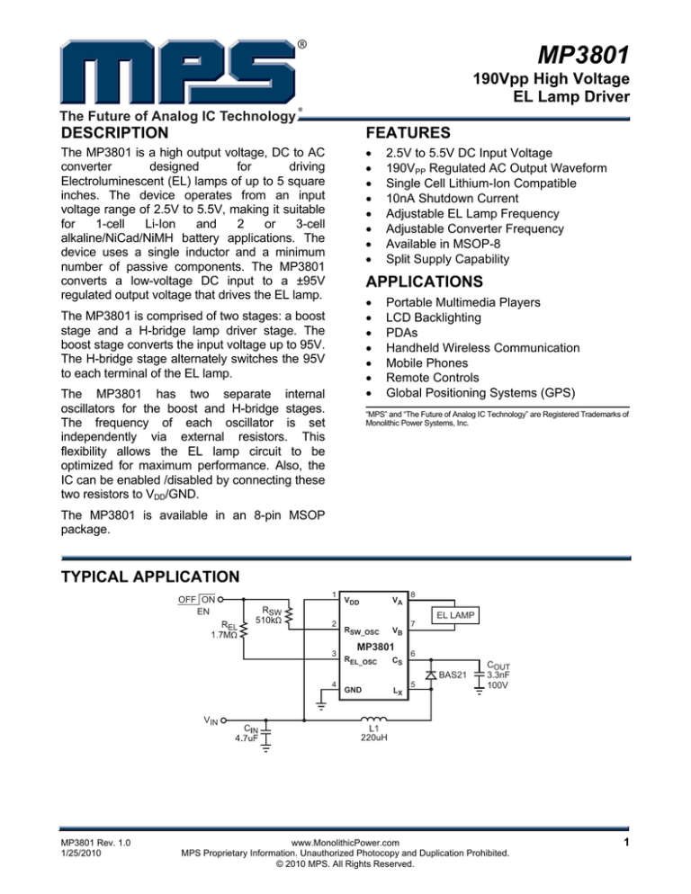
The MP3801 is comprised of two stages: a boost
stage and a H-bridge lamp driver stage. The
boost stage converts the input voltage up to 95V.
The H-bridge stage alternately switches the 95V
to each terminal of the EL lamp.
The MP3801 has two separate internal
oscillators for the boost and H-bridge stages.
The frequency of each oscillator is set
independently via external resistors. This
flexibility allows the EL lamp circuit to be
optimized for maximum performance. Also, the
IC can be enabled /disabled by connecting these
two resistors to VDD/GND.
Portable Multimedia Players
LCD Backlighting
PDAs
Handheld Wireless Communication
Mobile Phones
Remote Controls
Global Positioning Systems (GPS)
“MPS” and “The Future of Analog IC Technology” are Registered Trademarks of
Monolithic Power Systems, Inc.
The MP3801 is available in an 8-pin MSOP
package.
TYPICAL APPLICATION
OFF ON
EN
1
2
3
VDD
VA
RSW_OSC
VB
MP3801
REL_OSC
CS
8
7
EL LAMP
6
BAS21
4
GND
LX
5
COUT
3.3nF
100V
VIN
MP3801 Rev. 1.0
1/25/2010
www.MonolithicPower.com
MPS Proprietary Information. Unauthorized Photocopy and Duplication Prohibited.
© 2010 MPS. All Rights Reserved.
1
MP3801 – 190VPP HIGH VOLTAGE EL LAMP DRIVER
ABSOLUTE MAXIMUM RATINGS (1)
PACKAGE REFERENCE
Supply Voltage (VDD) .................. –0.5V to +6.0V
Output Voltage (VCS, VA, VB)...... –0.5V to +120V
All Other Pins...................... –0.5V to VDD + 0.3V
Junction Temperature...............................150°C
Lead Temperature ....................................260°C
Storage Temperature .............–65°C to +150°C
TOP VIEW
*
VDD
1
8
VA
RSW_OSC
2
7
VB
REL_OSC
3
6
CS
GND
4
5
LX
Recommended Operating Conditions
Part Number*
Package
Temperature
MP3801DH
MSOP8
–40°C to +85°C
(2)
Supply Voltage ............................... 2.5V to 5.5V
Lamp Drive Frequency (fEL) ..........60Hz to 1KHz
Switching Transistor Freq...... 50KHz to 200KHz
Operating Temperature .............–40°C to +85°C
Thermal Resistance (3)
θJA
θJC
MSOP8 .................................. 150 ..... 65... °C/W
For Tape & Reel, add suffix –Z (eg. MP3801DH–Z)
For RoHS Compliant Packaging, add suffix –LF
(eg. MP3801DH–LF–Z)
Notes:
1) Exceeding these ratings may damage the device.
2) The device is not guaranteed to function outside of its
operating conditions.
3) Measured on approximately 1” square of 1 oz copper.
ELECTRICAL CHARACTERISTICS
VIN = VDD = 3.0V, REL=1.7MΩ, RSW=510KΩ, TA = +25°C, unless otherwise noted.
Parameter
On Resistance of Switching
Transistor
Output Voltage Regulation
Peak to Peak Output Voltage
Input Low Voltage (Turn Off)
Input High Voltage (Turn On)
Shutdown Current
Input Supply Current
Symbol Condition
RDS(ON)
VCS
VA – VB
VEN-L
VEN-H
ISD
IVDD
Input Current Including Inductor
Current
IIN
EL Lamp Frequency
Switching Transistor Frequency
Switching Transistor Duty Cycle
fEL
fSW
D
Min
ISW = 100mA, VCS = 95V
Typ
Max
9
90
180
VEN = 0V
VA, VB Open, VEN = VIN
A 2kΩ resistor is series
with a 10nF capacitor
connected between VA
and VB
95
190
VDD – 0.6
VDD – 0.3
10
92
Ω
100
200
20
200
240
85
92
Units
V
V
V
V
nA
A
mA
274
Hz
KHz
%
Note:
4) Shutdown current is defined as the sum of currents going into VDD, VCS, and SW nodes.
MP3801 Rev. 1.0
1/25/2010
www.MonolithicPower.com
MPS Proprietary Information. Unauthorized Photocopy and Duplication Prohibited.
© 2010 MPS. All Rights Reserved.
2
MP3801 – 190VPP HIGH VOLTAGE EL LAMP DRIVER
PIN FUNCTIONS
Pin #
Name
1
VDD
2
RSW_OSC
3
REL_OSC EL Driver Frequency Setting Pin. Roughly, fEL=
4
5
GND
LX
6
CS
7
8
VB
VA
MP3801 Rev. 1.0
1/25/2010
Description
Supply Voltage.
Boost Converter Frequency Setting Pin. Refer the frequency setting curve in the typical
performance characteristics.
1.7MΩ × 240Hz
R EL
Ground. Connect the exposed pad to this pin.
Boost Converter Switching Pin. This pin connects to the N-Channel MOSFET drain.
Boost Converter Output. Put a 100V, NPO ceramic capacitor at this pin to stone the energy
transferred from the inductor.
Output Voltage B on EL Device.
Output Voltage A on EL Device.
www.MonolithicPower.com
MPS Proprietary Information. Unauthorized Photocopy and Duplication Prohibited.
© 2010 MPS. All Rights Reserved.
3
MP3801 – 190VPP HIGH VOLTAGE EL LAMP DRIVER
TYPICAL PERFORMANCE CHARACTERISTICS
280
275
270
265
260
2.0
3.0
4.0
5.0
30
250
25
200
20
fSW (kHz)
285
INPUT CURRENT (mA)
LAMP FREQUENCY (HZ)
290
15
0
6.0
50
VA
50V/div
VB
50V/div
VB
50V/div
VOUT
20V/div
VA
50V/div
VB
50V/div
VAB
100V/div
VAB
100V/div
2ms/div.
2ms/div.
VA
50V/div
VB
50V/div
VB
50V/div
2ms/div.
MP3801 Rev. 1.0
1/25/2010
VA
50V/div
VA
50V/div
VAB
100V/div
2ms/div.
VOUT
20V/div
VOUT
20V/div
VB
50V/div
0
300 350 400 450 500 550 600 650
0 0.5 1.0 1.5 2.0 2.5 3.0 3.5 4.0 4.5 5.0 5.5 6.0
VIN(V)
VA
50V/div
VOUT
20V/div
100
5
VOUT
20V/div
VAB
100V/div
150
10
VIN(V)
VOUT
20V/div
fsw vs. Rsw
Input current vs.
Input Voltage
Lamp Frequency vs.
Input Voltage
1ms/div.
www.MonolithicPower.com
MPS Proprietary Information. Unauthorized Photocopy and Duplication Prohibited.
© 2010 MPS. All Rights Reserved.
1ms/div.
4
MP3801 – 190VPP HIGH VOLTAGE EL LAMP DRIVER
TYPICAL PERFORMANCE CHARACTERISTICS (continued)
VOUT
20V/div
VA
50V/div
VB
50V/div
VOUT
20V/div
VOUT
20V/div
VA
50V/div
VA
50V/div
VB
50V/div
VB
50V/div
1ms/div.
1ms/div.
VOUT
20V/div
VA
50V/div
VB
50V/div
1ms/div.
MP3801 Rev. 1.0
1/25/2010
1ms/div.
VOUT
20V/div
VOUT
20V/div
VA
50V/div
VA
50V/div
VB
50V/div
VB
50V/div
1ms/div.
www.MonolithicPower.com
MPS Proprietary Information. Unauthorized Photocopy and Duplication Prohibited.
© 2010 MPS. All Rights Reserved.
1ms/div.
5
MP3801 – 190VPP HIGH VOLTAGE EL LAMP DRIVER
BLOCK DIAGRAM
L1
D1
VIN
CIN
REL
RSW
RSW_OSC
1
2
COUT
5 L
X
VDD
Switch
OSC
6
4
GND
Q3
+
--
Q1
EL
Driver
8
Ref
3
REL_OSC
EL
OSC
Q4
CS
VA
EL
Lamp
Q2
VB
7
Figure 1—Functional Block Diagram
MP3801 Rev. 1.0
1/25/2010
www.MonolithicPower.com
MPS Proprietary Information. Unauthorized Photocopy and Duplication Prohibited.
© 2010 MPS. All Rights Reserved.
6
MP3801 – 190VPP HIGH VOLTAGE EL LAMP DRIVER
PACKAGE INFORMATION
MSOP8
0.087(2.20)
0.099(2.50)
0.114(2.90)
0.122(3.10)
5
8
0.114(2.90)
0.122(3.10)
PIN 1 ID
(NOTE 5)
0.187(4.75)
0.199(5.05)
0.062(1.58)
0.074(1.88)
Exposed Pad
0.010(0.25)
0.014(0.35)
4
1
0.0256(0.65)BSC
BOTTOM VIEW
TOP VIEW
GAUGE PLANE
0.010(0.25)
0.030(0.75)
0.037(0.95)
0.043(1.10)MAX
SEATING PLANE
0.002(0.05)
0.006(0.15)
FRONT VIEW
NOTE:
0.181(4.60)
0.040(1.00)
0.016(0.40)
0.016(0.40)
0.026(0.65)
SIDE VIEW
0.100(2.54)
0.075(1.90)
0o-6o
0.004(0.10)
0.008(0.20)
1) CONTROL DIMENSION IS IN INCHES. DIMENSION IN BRACKET IS
IN MILLIMETERS.
2) PACKAGE LENGTH DOES NOT INCLUDE MOLD FLASH,
PROTRUSION OR GATE BURR.
3) PACKAGE WIDTH DOES NOT INCLUDE INTERLEAD FLASH OR
PROTRUSION.
4) LEAD COPLANARITY (BOTTOM OF LEADS AFTER FORMING)
SHALL BE 0.004" INCHES MAX.
5) PIN 1 IDENTIFICATION HAS HALF OR FULL CIRCLE OPTION.
6) DRAWING MEETS JEDEC MO-187, VARIATION AA-T.
7) DRAWING IS NOT TO SCALE.
0.0256(0.65)BSC
RECOMMENDED LAND PATTERN
NOTICE: The information in this document is subject to change without notice. Please contact MPS for current specifications.
Users should warrant and guarantee that third party Intellectual Property rights are not infringed upon when integrating MPS
products into any application. MPS will not assume any legal responsibility for any said applications.
MP3801 Rev. 1.0
1/25/2010
www.MonolithicPower.com
MPS Proprietary Information. Unauthorized Photocopy and Duplication Prohibited.
© 2010 MPS. All Rights Reserved.
7
