International Journal of Science, Engineering and Technology Research (IJSETR), Volume 4, Issue 5, May 2015
A Single-Phase 21-Level Inverter with Reduced
Switching Devices ACMLI for Different PWM
Techniques
Pushpendra kaurav, Praveen bansal
Abstract— Multilevel inverter is a power electronic device
and that is become more or more popularize over the years in
high-voltage high-power applications. Multilevel inverters have
unique structure which makes it possible to reach high voltages
with less harmonic content and lower EMI. The harmonic
content of the output voltage waveform decreases as the number
of output voltage increases. This paper presents a 21-level
multi-level inverter with Asymmetrical cascaded MLI topology.
This proposed multilevel inverter topology here is implemented
in single-phase with different pulse width modulation (PWM)
techniques, which requires less number of components, and gate
drive circuit as compared to other multilevel inverters. A
multicarrier PWM technique is used for multilevel inverter
topology to generate 21-level output phase voltage. Finally
simulation results of a 21-level multi-level inverter topology are
carried out using MATLAB/Simulink R2013a software version.
Index Terms— Multi-level inverter (MLIs), Asymmetrical
cascaded Voltage (ACMLI) topology and PWM techniques.
I.
INTRODUCTION
Multi-level power conversion is used to provide more than
two voltage level to achieve smoother and less distorted dc to
ac power conversion and it can generate a multiple-step
voltage waveform with less distortion, less switching
frequency and higher efficiency. Multilevel inverters have
become more popular over the years in high-power
high-voltage applications. Whereas conventional two level
inverter have some limitations in high-power high-voltage
applications due to switching losses and power ratings [1-3].
Multi-level inverter offers several advantages over two-level
inverter: it improves the output voltage waveform, reduced
(dv/dt) voltage stress on the load and also reduces
electromagnetic interference problems, but it has some
disadvantages when the number of voltage levels increases
such as; complex PWM controlling method, voltage
balancing problems are introduced and higher number of
semiconductor switches are required. Each switch requires a
separate gate driver circuit, therefore increasing the
complexity and size of the overall circuit. For this problem,
lower voltage rated switches can be used in multi-level
Manuscript received April, 2015.
Pushpendra kaurav, Department of electrical engineering, Madhav
Institute of Technology & Science, Gwalior, India, 9752289646,
Praveen bansal, Department of electrical engineering, Madhav Institute
of Technology & Science, Gwalior, India, 9827577549.
inverter instead of higher number of semiconductor switches
which can be used to minimized cost of the semiconductor
switches as compared to two level inverters [4].
There are different conventional multi-level inverters
topology mainly classified as Diode clamped multilevel
inverter (DCMLI) [5], Flying capacitor inverter (FCMLI),
cascaded H-bridge multilevel inverter (CHBMLI). In 1981 a
three level diode clamped multilevel inverter schemes
proposed by nabae [6]. The flying capacitor inverter structure
is similar to that of diode clamped inverter but the main
difference is that instead of clamping diodes, flying capacitors
are used.
The control method of cascaded H Bridge multilevel is more
convenient than other multilevel inverter because it doesn‟t
have any clamping diode and flying capacitor. Cascaded
multilevel inverter reaches higher reliability [7]. The
cascaded inverter is used for large automotive electric drives.
However, the requirement of more number of switches and
separate dc source for each cell becomes a problem especially
at higher level. Cascaded h-bridge multilevel inverter consists
of separate dc links for each h-bridge cell so it is easily
controllable. Cascaded h-bridge multilevel inverter has some
drawback that by increasing the number of voltage levels
numbers of switching devices given by 2(N+1) also increase
[8].
This paper proposes a 21-level multi-level inverter with
ACMIL topology which requires less number of switches and
gate driver circuits as compared to conventional multilevel
inverters. The proposed multilevel inverter topology [9] here
is implemented in single-phase with different PWM
techniques. The pulse-width modulation (PWM) control is
the most efficient technique of controlling output voltage
within the inverters. The carrier based PWM schemes used
for multilevel inverters is the most efficient method, realized
by the intersection of a modulating signal with triangular
carrier waveform. The paper tries to prove that ACMIL
topology is better than conventional multilevel inverters
topology in terms of their number of components and THD.
II. PROPOSED TOPOLOGY
A single DC supply to output voltages two level 0 and V.
It is used two switches S1 and S2. If switch S1 is ON, output
voltage are V and switch S2 is ON output voltage are zero.
Switches S1 and S2 are OFF simultaneously to avoid the
occurrence of short circuit across the DC supply.
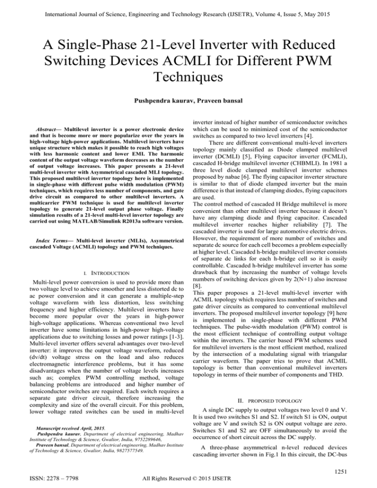
A three-phase asymmetrical n-level reduced devices
cascading inverter shown in Fig.1 In this circuit, the DC-bus
1251
ISSN: 2278 – 7798
All Rights Reserved © 2015 IJSETR
International Journal of Science, Engineering and Technology Research (IJSETR), Volume 4, Issue 5, May 2015
voltage is split into each cell. Which are connected in series
and desired number of level can be achieved by series
connection of switch.
S1
V
S1
V
S2
S2
S3
S3
S11
S9
2V
S4
S4
LOAD
S5
S12
LOAD
S10
S5
3V
S11
S9
2V
S12
S10
S6
3V
S7
S8
4V
S6
S7
S7
4V
nV
S8
S8
Fig.1 Proposed n-level asymmetrical reduced device cascaded MLI
The proposed ACMLI topology for 21-level inverter
requires twelve semiconductor switches and four isolated dc
sources shown in Fig 2 [9] which separates output voltage in
two parts. One part is called level generation part (left side)
and is responsible for level generating in positive polarity &
negative polarity. The other part is called polarity generation
part (right side) and is responsible for generating the polarity
of the output voltage. This topology combines the two parts
(left part and right part) to generate the multi-level output
voltage waveform.
The main purpose of this proposed ACMLI topology is to
control the EMI, minimize the total harmonic distortion with
different PWM techniques and it also minimizes power
semiconductor switches than conventional multilevel
inverter. For a conventional single-phase 21-level inverter, it
uses 40 switches, whereas the proposed topology uses only 12
switches.
Here proposed topology is also used for three-phase MLI
with the same principle. The proposed topology is a
symmetrical topology because all the values of all voltage
sources are equal. Therefore, it does not have
voltage-unbalancing due to fixed dc voltage values. In
comparison with a cascade h-bridge inverter topology,
proposed topology requires only one-third of isolated power
supplies used in a cascade-type inverter [10]. The operation of
the proposed topology has been discussed in detail and has
been verified with the help of simulations [11].
Fig.2 Proposed single-phase asymmetrical cascade 21-level inverter for line
to ground voltages
A. OPERTION FOR THE PROPOSED TOPOLOGY
Operation of the proposed 21-level MLI with asymmetrical
cascaded topology can be easily explained with the help of
fig. 2 and table I. When switches S1, S3, S5 and S7 are turned
“on” the output voltage will be “10Vdc” (i.e., level +10). The
output voltage will be “9Vdc” (i.e., level +9) when switches
S2, S3, S5 and S7 are turned “on”. When S1, S4, S5 and S7
switches are turned “on” the output voltage will be “8Vdc”
(i.e., level +8). When switches S2, S4, S5 and S7 are turned on
the output voltage will be “7Vdc” (i.e., level +7). When
switches S1, S3, S5 and S8 are turned “on” the output voltage
will be “6Vdc” (i.e., level +6). The output voltage will be
“5Vdc” (i.e., level +5) when switches S1, S4, S6 and S7 are
turned “on”. When S2, S4, S6 and S7 switches are turned “on”
the output voltage will be “4Vdc” (i.e., level +4). When
switches S1, S3, S6 and S8 are turned on the output voltage will
be “3Vdc” (i.e., level +3). The output voltage will be “2Vdc”
(i.e., level +2) when switches S2, S3, S6 and S8 are turned
“on”. When S1, S4, S6 and S8 switches are turned “on” the
output voltage will be “Vdc” (i.e., level +1). When switches
S2, S4, S6 and S8 are turned “on” the output voltage is zero
(i.e., level 0). Switches S9, S10, S11 and S12 are used for a
complementary pair. When S10 and S11 are turned “on”
together, positive half cycle (level; +1, +2, +3, and +4) can be
generated and when S9 and S12 are turned “on” together,
negative half cycle (level; -1, -2, -3, and -4) can be generated
across load.
1252
ISSN: 2278 – 7798
All Rights Reserved © 2015 IJSETR
International Journal of Science, Engineering and Technology Research (IJSETR), Volume 4, Issue 5, May 2015
TABLE.I
VOLTAGE
LEVEL
+10
+9
+8
+7
+6
+5
+4
+3
+2
+1
0
-1
-2
-3
-4
-5
-6
-7
-8
-9
-10
SWITCHING STATE
S1 S 2 S3 S4 S5
1
0
1
0
1
0
1
1
0
1
1
0
0
1
1
0
1
0
1
1
1
0
1
0
1
1
0
0
1
0
0
1
0
1
0
1
0
1
0
0
0
1
1
0
0
1
0
0
1
0
0
1
0
1
0
1
0
0
1
0
0
1
1
0
0
1
0
1
0
0
0
1
0
1
0
1
0
0
1
0
1
0
1
0
1
0
1
0
1
1
1
0
0
1
1
0
1
1
0
1
1
0
1
0
1
S6
0
0
0
0
0
1
1
1
1
1
1
1
1
1
1
1
0
0
0
0
0
S7
1
1
1
1
0
1
1
0
0
0
0
0
0
0
1
1
0
1
1
1
1
S8
0
0
0
0
1
0
0
1
1
1
1
1
1
1
0
0
1
0
0
0
0
S9
1
1
1
1
1
1
1
1
1
1
1
0
0
0
0
0
0
0
0
0
0
S10
1
1
1
1
1
1
1
1
1
1
1
0
0
0
0
0
0
0
0
0
0
S11
0
0
0
0
0
0
0
0
0
0
0
1
1
1
1
1
1
1
1
1
1
S12
0
0
0
0
0
0
0
0
0
0
0
1
1
1
1
1
1
1
1
1
1
OUTPUT
VOLTAGE
10V
9V
8V
7V
6V
5V
4V
3V
2V
V
0
-V
-2V
-3V
-4V
-5V
-6V
-7V
-8V
-9V
-10V
S1
B. Mode Of Operation
V
S2
S1
S3
V
S2
2V
2V
S11
S9
S4
S3
LOAD
S5
S11
S9
S4
S12
S10
LOAD
3V
S5
S12
S6
S10
S7
3V
S6
S8
4V
S7
Level -1
Fig (c)
S8
4V
Level 0
S1
Fig (a)
S1
V
V
S2
S2
S3
S3
2V
S11
S9
S4
S1 1
S9
2V
S4
LOAD
LOAD
S5
S5
3V
S12
S6
S 12
S10
3V
S1 0
S6
S7
S7
4V
S8
4V
S8
Level +1
Level +2
Fig (b)
Fig (d)
1253
ISSN: 2278 – 7798
All Rights Reserved © 2015 IJSETR
International Journal of Science, Engineering and Technology Research (IJSETR), Volume 4, Issue 5, May 2015
S1
V
S1
V
S2
S3
2V
S2
S3
S11
S9
S4
S5
S4
LOAD
S 12
3V
S5
S10
S6
3V
S7
4V
S10
S9
S11
S6
4V
S
8
Level -2
Level - 4
Fig (h)
Fig (e)
S1
S1
S2
V
S3
S2
S3
S1 1
S9
2V
S 12
S7
S8
V
S11
S9
2V
LOAD
S4
2V
S4
LOAD
LOAD
S5
3V
S 12
S1 0
S5
S12
S10
S6
3V
S6
S7
S7
4V
S8
4V
S8
Level +3
Level +5
Fig (f)
S1
Fig (i)
S1
V
S2
V
S2
S3
S3
2V
S11
S9
S4
LOAD
S5
S12
2V
LOAD
S10
S5
3V
S11
S9
S4
S 12
S10
S6
3V
S6
S7
S7
4V
S8
4V
S8
Level -3
Level -5
Fig (j)
Fig (g)
S1
S1
V
S2
V
S2
S3
S3
S1 1
S9
2V
S4
S11
S9
2V
LOAD
S4
LOAD
S5
3V
S 12
S1 0
S5
S 12
S10
S6
3V
S6
S7
S7
4V
S8
4V
Level +4
S8
Level +6
Fig (k)
Fig (g)
1254
ISSN: 2278 – 7798
All Rights Reserved © 2015 IJSETR
International Journal of Science, Engineering and Technology Research (IJSETR), Volume 4, Issue 5, May 2015
S1
S1
V
V
S2
S2
S3
S3
S11
S9
2V
S4
S11
S9
V
S4
LOAD
LOAD
S5
3V
S 12
S5
S10
S6
V
S10
S6
S7
4V
S 12
S7
S8
V
S8
Level -6
Level -8
Fig (l)
Fig (p)
S1
S1
V
S2
V
S2
S3
S3
S1 1
S9
2V
S4
LOAD
S5
S 12
S4
LOAD
S5
3V
S11
S9
2V
S1 0
S 12
S10
S6
3V
S6
S7
S7
4V
S8
4V
S8
Level +7
Level +9
Fig (q)
Fig (m)
S1
S1
V
S2
V
S2
S3
S3
2V
S 11
S9
S4
S11
S9
2V
LOAD
S4
LOAD
S5
3V
S12
S10
S5
S 12
S10
S6
3V
S6
S7
S7
4V
S8
4V
S8
Level -7
Level -9
Fig (r)
Fig (n)
S1
V
S1
V
S2
S3
S3
S11
S9
2V
S2
S1 1
S9
2V
S4
S4
LOAD
LOAD
S5
S5
S 12
3V
3V
S 12
S1 0
S10
S6
S6
S7
S7
4V
4V
S8
S8
Level +10
Level +8
Fig (o)
Fig (s)
1255
ISSN: 2278 – 7798
All Rights Reserved © 2015 IJSETR
International Journal of Science, Engineering and Technology Research (IJSETR), Volume 4, Issue 5, May 2015
S1
V
multistep output waveform. MLI with N levels requires
(N-1) triangular carriers. In phase shifted PWM, all the
triangular carriers have same frequency and same peak to
peak amplitude.
S2
S3
2V
S11
S9
S4
LOAD
S5
S12
3V
IV. SIMULATION RESULTS
S10
S6
S7
4V
S8
Level -10
Fig (t)
Fig.3 Fig (a), Fig (b), Fig (c), Fig (d), Fig (e), Fig (f), Fig (g), Fig (h), and Fig
(i), Fig (j), Fig (k), Fig (l), Fig (m), Fig (n), Fig (o), Fig (p), Fig (q), Fig (r),
Fig (s), and Fig (t), are Switching combination of 21-level MLI.
The Fig.1 & 2 shows the proposed topology model of
single-phase n-level & single-phase 21-level ACMLI. Table
II shows THD comparison between different PWM
techniques. The simulation parameters are as following R =
10 ohms, L = 10mH, and dc source voltage is 400V; Carrier
signal frequency is 1 kHz. In this paper, four PWM techniques
are used PD, POD, APOD, PS, VF and CO with different
modulation index (Ma). For Ma = 1.0, and Mf = 20,
corresponding (%) THD are PS = 5.54, PD = 5.78, POD =
6.01, APOD = 5.10, shown in Fig. 6.1 – 6.6. The harmonic
spectrum is carried out by using the FFT analysis in
MATLAB/Simulink.
100
III. MODULATION STRATEGIE
80
60
Multilevel Converter
Multicarrier PWM
output current
40
20
0
-20
-40
-60
Level-Shifted
PWM
Phase-Shifted
PWM
Carrier Overlapping
PWM
Variable Frequency
PWM
-80
-100
0
0.01
0.02
0.03
0.04
0.05
0.06
0.07
0.08
Time
Fig.4 Single-Phase current by PSPWM for 24-level inverter with R-L load
1000
800
600
Phase Opposition
Disposition PWM
400
output voltage
Phase Disposition
PWM
Alternate Phase
Opposition Disposition
PWM
200
0
-200
-400
There are different pulse width modulation strategies as given
below [12-13].
-600
-800
-1000
0
0.01
0.02
0.03
0.04
0.05
0.06
0.07
0.08
Time
A. Phase disposition pulse width modulation (PD PWM):In phase disposition pulse width modulation strategy, where
all carrier waveforms are in same phase.
Fig.5 Single-Phase Voltage by PSPWM for 24-level inverter with R-L load
B. Phase opposition disposition pulse width modulation
(POD PWM):- In phase opposition disposition pulse width
modulation strategy, where all carrier waveforms above
zero reference are in phase and below zero reference are
1800 out of phase.
C. Alternate phase opposition disposition pulse width
modulation (APOD PWM):- In alternate phase opposition
disposition PWM scheme where every carrier waveform is
in out of phase with its neighbor carrier by 1800.
D. Phase-shifted pulse width modulation (PS PWM):- A
carrier phase shifted PWM for multi-level inverter is used to
generate the stepped multi-level output voltage waveform
with lower % THD. In proposed, before implementing the
Multicarrier PWM Techniques, the gating signals of
multi-level inverter switches are generated by comparing
sinusoidal reference wave with triangular carrier waves at
specific intervals of time producing the characteristic
Fig. 6.1: FFT analysis by PDPWM for R-L load (Ma=1.0, Mf=20).
Fig. 6.2.: FFT analysis by PODPWM for R-L load (Ma=1.0, Mf=20).
1256
ISSN: 2278 – 7798
All Rights Reserved © 2015 IJSETR
International Journal of Science, Engineering and Technology Research (IJSETR), Volume 4, Issue 5, May 2015
Modulatio
n
Index
Fig. 6.3: FFT analysis by APODPWM for R-L load (Ma=1.0, Mf=20).
1.1
PS
PWM
%TH
D
6.24
PD
PWM
%TH
D
5.75
POD
PWM
%TH
D
5.75
APOD
PWM
%TH
D
4.70
VF
PWM
%TH
D
5.70
CO
PWM
%TH
D
8.09
1.0
5.54
5.78
6.01
5.10
5.57
8.69
0.9
6.43
6.12
5.99
6.28
6.23
10.20
0.8
7.31
6.99
6.82
6.44
6.60
11.97
TABLE. III COMPARISON OF THE PROPOSED AND CONVENTIONAL MLI
main switching
Devices
diodes
DC bus
balancing
capacitors
DCMIL
FCMLI
Proposed
Inverter
40
40
12
40
20
0
40
20
200
12
4
0
2000
Fig. 6.4: FFT analysis by PSPWM for R-L load (Ma=1.0, Mf=20).
Number of 3 phase components
1800
1600
NPC
Flying
Cascade
ACMLI
1400
1200
1000
800
600
400
200
0
5
10
15
20
25
Number of output voltage levels
Fig.7 Required number of single phase components for different multi-level
inverter topologies.
Fig. 6.5: FFT analysis by VFPWM for R-L load (Ma=1.0, Mf=20).
Fig. 7 shows the required number of single phase components
for different multilevel inverter topologies. So it is clearly
shows that the proposed ACMLI topology is requires less
number of components than other conventional topologies so
as the voltage level increases the number of components will
decreases particularly for higher voltage levels [14-15].
V. CONCLUSION
Fig. 6.6: FFT analysis by COPWM for R-L load (Ma=1.0, Mf=20).
TABLE. II THD ANALYSIS B/W DIFFERENT PWM TECHNIQUES FOR 21-LEVEL
MLI
In this paper, a 21-level multi-level inverter using
Asymmetrical cascaded MLI topology is proposed with
different PWM techniques and proposed MLI topology with
different PWM techniques is used to generate 21-level output
phase voltage. It is proved that, the proposed work of Single
phase 21-level MLI output voltage total harmonics distortion
is reduced and improve the efficiency of system compare with
different conventional topologies of single phase and
three-phase 21-level MLI. Harmonic analysis carried out
using Mat Lab R2013a version software. This proposed MLI
topology requires less number of components as compared to
1257
ISSN: 2278 – 7798
All Rights Reserved © 2015 IJSETR
International Journal of Science, Engineering and Technology Research (IJSETR), Volume 4, Issue 5, May 2015
conventional MLI inverters. Simulation results show the
performance of single-phase MLI with different PWM
techniques.
REFERENCES
[1]
[2]
[3]
[4]
[5]
[6]
[7]
[8]
[9]
[10]
[11]
[12]
[13]
[14]
[15]
Rodriguez, J., Jih-Sheng, L., Fang Zheng, P.: „Multilevel inverters: a
survey of topologies, controls, and applications‟, IEEE Trans. Ind.
Electron., 2002, 49, pp. 724–738.
Colak, I., Kabalci, E., Bayindir, R.: „Review of multilevel voltage
source inverter topologies and control schemes‟, Energy Convers.
Manage., 2011, 52, (2), pp. 1114–1128.
J. S. Lai and F. Z. Peng, “Multilevel converters – A new breed of power
converters,” IEEE Trans. Ind. Applica, vol. 32, no. 3, pp. 509-517,
May/June 1996.
L. Tolbert, F.-Z. Peng, and T. Habetler, “Multilevel converters for large
electric drives,” IEEE Trans. Ind. Applicat., vol. 35, pp. 36–44,
Jan./Feb. 1999.
Nabe, I. Takahashi and H. Akagi. “A new neutral point clamped PWM
inverter.” IEEE Trans. Ind. Applicat. Vol. 1A-17, pp 518- 523, sep.
/oct. 1981.
X.Yuan and I.Barbi, "Fundamentals of a New Diode
ClampingMultilevel Inverters", IEEE Transaction Power Electron.,
Vol.15, No.4, 2000, pp.711-718.
B. M. Song, S. Gurol, C. Y. Jeong, D. W. Yoo, and J. S. Lai, “A
soft-switching high-voltage active power filter with flying capacitors
for urban maglev system applications,” in Conf. Rec. IEEE-IAS Annu.
Meeting, Chicago, IL, Sept. 2001, pp. 1461–1469.
K. A. Corzine, M. W. Wielebski, F. Z. Peng, and J. Wang, “Control of
Cascaded Multilevel Inverters,” IEEE Trans. power electron, vol.19,
no.3, pp. 732-738, May 2004.
Kiruthika, C., Ambika, T., Seyezhai, R.: „Implementation of digital
control strategy for asymmetric cascaded multilevel inverter‟.
International Conference on Computing, Electronics and Electrical
Technologies (ICCEET), 2012, pp. 295–300.
Baier, C.R., Guzman, J.I., Espinoza, J.R., Perez, M.A., Rodriguez,
J.R.: „Performance evaluation of a multi cell topology implemented
with single-phase non regenerative cells under unbalanced supply
voltages‟, IEEE Trans. Ind. Electron., 2007, 54, pp. 2969–2978.
S. Mariethoz and A.C. Rufer. Design and control of asymmetrical
multilevel inverters. IECON’02, November 2002.
M. Manjrekar and G. Venkataramanan, “Advanced topologies and
modulation strategies for multilevel inverters,” in Proc. IEEE
PESC’96, Baveno, Italy, June 1996, pp. 1013–1018.
D. G. Holmes and B. P. McGrath, “Opportunities for harmonic
cancellation with carrier-based PWM for two-level and multilevel
cascaded inverters,” IEEE Trans. Ind. Applicat., vol. 37, pp. 574–582,
Mar./Apr. 2001.
V. G. Agelidis and M. Calais, “Application specific harmonic
performance evaluation of multicarrier PWM techniques,” in Proc.
IEEE PESC’98, Fukuoka, Japan, May 1998, pp. 172–178.
Gupta, K.K.; jain, S., “A novel universal control scheme for multilevel
inverter,” Power Electronics Machine And Drive (PEMD 2012),
6thIET International Conference on , vol., no., pp.1,6 27-29 March
2012
First Author
Pushpendra kaurav was born on July 1, 1991. His graduation in
Electrical Engineering from the Institute of Information Technology &
Management (IITM) in Gwalior and pursuing M.E at Madhav Institute of
Technology and Science (MITS) in Gwalior.
Second Author
Praveen Bansal obtained his bachelor of Engineering (Hon‟s) in
Electrical Engineering from Madhav Institute of Technology and
Science(MITS) ,Gwalior in 2009,MTech degree in Electrical Drives from
Maulana Azad National Institute of Technology in 2012,Currently he is an
Assistant Professor at MITS, Gwalior. His area of interests includes
multilevel Inverters, Induction motor modeling, and PWM techniques.
1258
ISSN: 2278 – 7798
All Rights Reserved © 2015 IJSETR


