Set No.1
advertisement

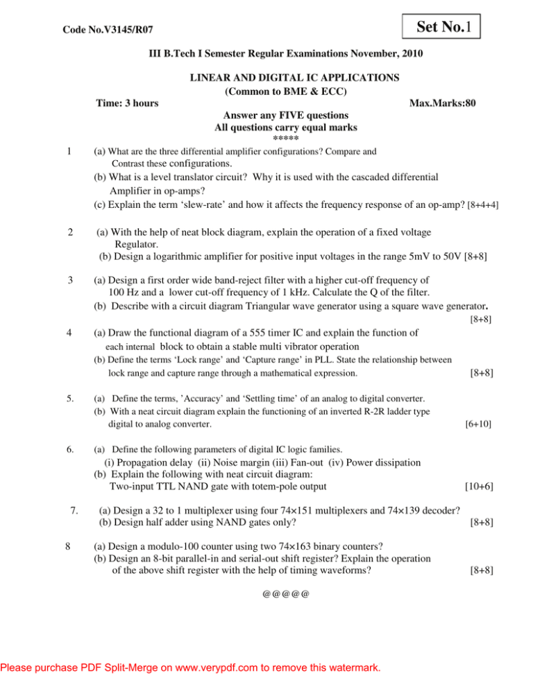
Set No.1 Code No.V3145/R07 III B.Tech I Semester Regular Examinations November, 2010 LINEAR AND DIGITAL IC APPLICATIONS (Common to BME & ECC) Time: 3 hours Max.Marks:80 Answer any FIVE questions All questions carry equal marks ***** 1 (a) What are the three differential amplifier configurations? Compare and Contrast these configurations. (b) What is a level translator circuit? Why it is used with the cascaded differential Amplifier in op-amps? (c) Explain the term ‘slew-rate’ and how it affects the frequency response of an op-amp? [8+4+4] 2 (a) With the help of neat block diagram, explain the operation of a fixed voltage Regulator. (b) Design a logarithmic amplifier for positive input voltages in the range 5mV to 50V [8+8] 3 (a) Design a first order wide band-reject filter with a higher cut-off frequency of 100 Hz and a lower cut-off frequency of 1 kHz. Calculate the Q of the filter. (b) Describe with a circuit diagram Triangular wave generator using a square wave generator. [8+8] 4 (a) Draw the functional diagram of a 555 timer IC and explain the function of each internal block to obtain a stable multi vibrator operation (b) Define the terms ‘Lock range’ and ‘Capture range’ in PLL. State the relationship between lock range and capture range through a mathematical expression. 5. 6. (a) Define the terms, ’Accuracy’ and ‘Settling time’ of an analog to digital converter. (b) With a neat circuit diagram explain the functioning of an inverted R-2R ladder type digital to analog converter. 8 [6+10] (a) Define the following parameters of digital IC logic families. (i) Propagation delay (ii) Noise margin (iii) Fan-out (iv) Power dissipation (b) Explain the following with neat circuit diagram: Two-input TTL NAND gate with totem-pole output 7. [8+8] [10+6] (a) Design a 32 to 1 multiplexer using four 74×151 multiplexers and 74×139 decoder? (b) Design half adder using NAND gates only? [8+8] (a) Design a modulo-100 counter using two 74×163 binary counters? (b) Design an 8-bit parallel-in and serial-out shift register? Explain the operation of the above shift register with the help of timing waveforms? @@@@@ Please purchase PDF Split-Merge on www.verypdf.com to remove this watermark. [8+8] Set No.2 Code No.V3145/R07 III B.Tech I Semester Regular Examinations November, 2010 LINEAR AND DIGITAL IC APPLICATIONS (Common to BME & ECC) Time: 3 hours Max.Marks:80 Answer any FIVE questions All questions carry equal marks ***** 1 ` Explain in detail all dc & ac characteristics of an ideal OP-amp with relevant expressions [16] 2 (a) Draw and explain the internal block schematic of an operational amplifier. (b) What is active load? Where it is used and why? [8+8] 3 (a) Draw the circuits and explain the working of i)Voltage to current converter ii)Current to voltage converter (b) Draw a circuit using Op-amp which can work as adder (inverting & noninverting) and explain how it works. [5+5] 4. (a) Design a narrow band pass filter with butter worth response for the following specifications f0 = 10 kHz, Q = 10 and pass band gain 10.. (b) List out the applications of VCO 566. [10+6] 5. (a) Explain the operation of a Successive Approximation type analog to digital converter. (b) Calculate the no. of bits required to represent a full scale voltage of 10V with a resolution of 5mV approximately. 6. (a) Distinguish between a stable, bi stable and mono stable multi vibrators. (b) Draw the circuit of a 565 PLL IC and explain its working. 7. ( a) With the help of a neat diagram, explain the working of a two –input CMOS NAND gate. What is the advantage of active load? (b) How is propagation delay improved in totem-pole TTL and CMOS logic? (c) Explain the interfacing of a TTL gate driving CMOS gates and vice versa. 8. (a) Implement a 16:1 multiplexer using 4:1 multiplexers ICs and explain. [6+6+4] (b) Draw the circuit of a 3 to 8 decoder and explain its operation. How this can be used as a DEMUX. (c) Write briefly on Static bi-polar RAM cell @@@@@ Please purchase PDF Split-Merge on www.verypdf.com to remove this watermark. [6] [10+6] [8+8] [6+4+6] Set No.3 Code No.V3145/R07 III B.Tech I Semester Regular Examinations November, 2010 LINEAR AND DIGITAL IC APPLICATIONS (Common to BME & ECC) Time: 3 hours 1 2 Max.Marks:80 Answer any FIVE questions All questions carry equal marks ***** (a) Discuss about dc analysis of Dual input balanced output amplifier. [8+8] (b) A 741 Op-amp is used as an inverting amplifier with a gain of 50. The voltage gain vs frequency curve of 741 is flat up to 20 KHz. What is the maximum peak to peak input signal that can be applied without distorting the output. (a) What is an instrumentation amplifier? What are the advantages? Derive an expression for the transfer function of an instrumentation amplifier. (b) Explain the operation of an Op-amp based mono stable multi vibrator. [10+6] 3 (a) Compare Butterworth, Chebyshev, and Bessel filter circuits. [8+8] (b) It is desired to get triangular waveform output from square wave input of 5 kHzs. Draw the circuit and give values of R and C. Explain the operation. 4 (a) Explain the operation of Schmitt trigger using 555 timer with its circuit diagram (b) Draw the circuit of a 565 PLL IC and explain its working. 5 (a) Define the terms, ‘Resolution’, ‘Linearity’, and ‘Conversion time’ of an analog to [8+8] digital converter. (b) Describe in detail the operation of a dual slope Analog to digital converter and explain its merits and demerits. 6 (a) Explain the basic ECL OR/NOR gate with a neat circuit diagram. Why does the ECL family have the lowest propagation delay of all logic families? (b) Explain the working of basic TTL NAND gate with a neat diagram. Explain the following three types of output configuration. (i) Open collector output (ii) Totem-pole output (iii) Tri-state output 7 (a) Design an 8:1 multiplexer using NAND gates only. (b) Design full adder using NOR gates only (c) Write briefly on priority encoder 8 (a) Design and implement a Mod-6 synchronous counter using J-K flip-flop. [6+6+4] (b) Design 4 bit left shift register with serial in and parallel out facility. Show the output waveform of each flip flop output. (c) Explain the functional behavior of Static RAM cell @@@@@ Please purchase PDF Split-Merge on www.verypdf.com to remove this watermark. [8+8] [8+8] [6+6+4] Set No.4 Code No.V3145/R07 III B.Tech I Semester Regular Examinations November, 2010 LINEAR AND DIGITAL IC APPLICATIONS (Common to BME & ECC) Time: 3 hours 1 Max.Marks:80 Answer any FIVE questions All questions carry equal marks ***** (a) Briefly describe the important op-amp parameters. (b) Draw and explain the working of an op amp with offset-voltage compensating network. (c) Explain frequency compensation techniques used in op-amps. [8+4+4] 2. (a) Describe the principle of operation of a peak detector with wave forms. (b) Design a Schmitt trigger circuit using an Op-amp to set UTP = 4 V and LTP = -2V; supply voltages of ± 15 V. Sketch the hysteresis loop. [8+8] 3. (a) Draw the circuit and explain the operation of Wien- bridge oscillator. (b) Draw the first order low pass Butterworth filter and analyze the same by deriving the gain and phase angle equations. [8+8] 4. (a) Describe the 555 timer mono stable multi vibrator applications in i) Frequency divider ii) Pulse width modulation (b) Define the terms: (1) free-running frequency f0, (2) lock range, (3) capture range, and (4) pull-in time, pertaining to PLL (a) Write a short note on performance specifications of a digital to analog converter. (b) Explain the operation of a counter type of analog to digital converter. (c) Compare weighted resistor type and R-2R-ladder type DACs. [8+8] 5. [6+6+4] 6. (a) What are the desirable features of CMOS gates? [5+5+6] (b) With a neat diagram, explain the operation of a two-inputs CMOS NOR gate. (c) Define the following terms: i) Fan-in ii). Fan-out iii) Current sink & Current source. 7. (a) Explain with a neat circuit diagram the tri-state TTL gate. How can the tri-state circuit outputs be connected together to form a data bus so that each output can be switched onto the bus wire? (b) Implement the following Boolean function using 8:1 multiplexer F(ABCD) = ABD + ACD + BCD + ACD (c) Design a full-subtractor using 3:8 decoders. [4+6+6] (a) Draw logical diagram of a 4-bit shift register. Explain how shift-left and Shift-right operations are performed. (b) Explain the operation of edge triggered T flip-flop. @@@@@ [8+8] 8. Please purchase PDF Split-Merge on www.verypdf.com to remove this watermark.

