MX884
High-Side Current Monitor
With 10-Bit Serial Digital Output
INTEGRATED CIRCUITS DIVISION
Features
Description
•
•
•
•
•
•
•
The MX884 targets power management applications
where high noise immunity and low cost are primary
requirements. Its integrated 10-bit ADC provides high
resolution, making it ideal for current monitoring
systems. The MX884 enables digital power
management, in which a microcontroller can readily
monitor the current in a system, and perform other
control functions in power systems and motion control
products.
3V to 60V Operating Voltage Range
Integrated 10-bit ADC
3-Wire Serial Interface
Microcontroller Compatible
Low Power
Minimum External Components
TSOT23 RoHS Compliant Package
Applications
•
•
•
•
•
Lighting Management
Current Shunt Measurement
Remote Sensing
Battery Monitoring
Microprocessor Controlled Power Management
Pb
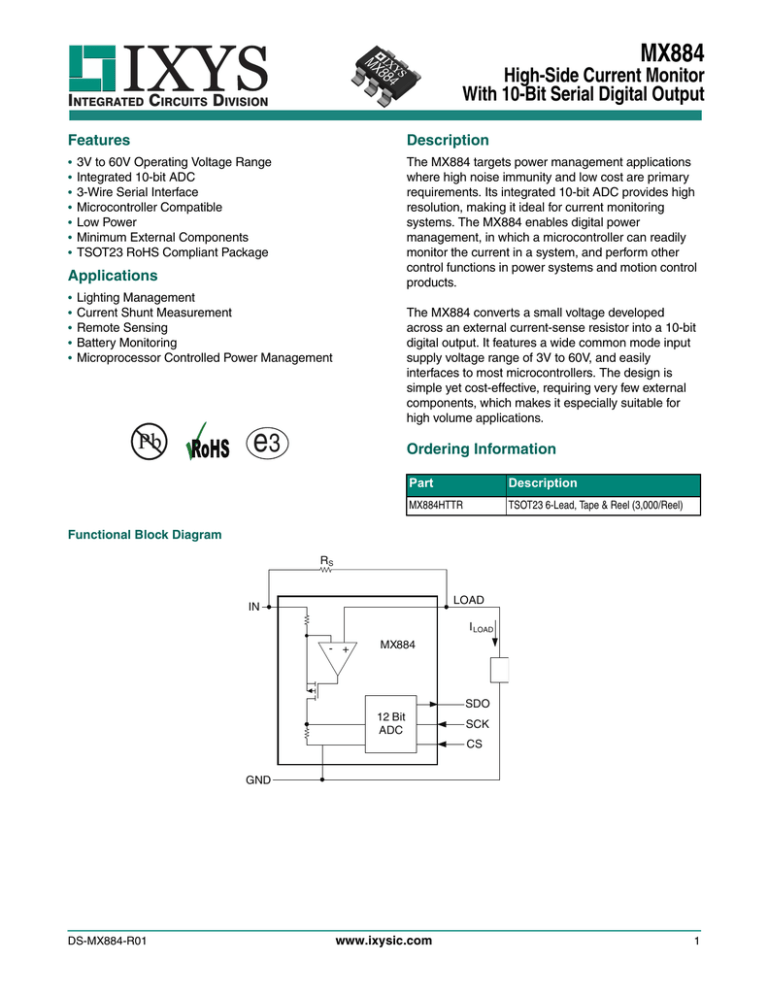
The MX884 converts a small voltage developed
across an external current-sense resistor into a 10-bit
digital output. It features a wide common mode input
supply voltage range of 3V to 60V, and easily
interfaces to most microcontrollers. The design is
simple yet cost-effective, requiring very few external
components, which makes it especially suitable for
high volume applications.
e3
Ordering Information
Part
Description
MX884HTTR
TSOT23 6-Lead, Tape & Reel (3,000/Reel)
Functional Block Diagram
RS
LOAD
IN
I LOAD
- +
MX884
SDO
12 Bit
ADC
SCK
CS
GND
DS-MX884-R01
www.ixysic.com
1
MX884
INTEGRATED CIRCUITS DIVISION
1. Specifications . . . . . . . . . . . . . . . . . . . . . . . . . . . . . . . . . . . . . . . . . . . . . . . . . . . . . . . . . . . . . . . . . . . . . . . . . . . . . . . . . . . . . . . . . . . . . .
1.1 Package Pinout . . . . . . . . . . . . . . . . . . . . . . . . . . . . . . . . . . . . . . . . . . . . . . . . . . . . . . . . . . . . . . . . . . . . . . . . . . . . . . . . . . . . . . . . .
1.2 Pin Description. . . . . . . . . . . . . . . . . . . . . . . . . . . . . . . . . . . . . . . . . . . . . . . . . . . . . . . . . . . . . . . . . . . . . . . . . . . . . . . . . . . . . . . . . .
1.3 Absolute Maximum Ratings . . . . . . . . . . . . . . . . . . . . . . . . . . . . . . . . . . . . . . . . . . . . . . . . . . . . . . . . . . . . . . . . . . . . . . . . . . . . . . . .
1.4 DC Electrical Characteristics . . . . . . . . . . . . . . . . . . . . . . . . . . . . . . . . . . . . . . . . . . . . . . . . . . . . . . . . . . . . . . . . . . . . . . . . . . . . . . .
3
3
3
3
3
2. Functional Description . . . . . . . . . . . . . . . . . . . . . . . . . . . . . . . . . . . . . . . . . . . . . . . . . . . . . . . . . . . . . . . . . . . . . . . . . . . . . . . . . . . . . . . 4
3. Manufacturing Information . . . . . . . . . . . . . . . . . . . . . . . . . . . . . . . . . . . . . . . . . . . . . . . . . . . . . . . . . . . . . . . . . . . . . . . . . . . . . . . . . . . .
3.1 Moisture Sensitivity . . . . . . . . . . . . . . . . . . . . . . . . . . . . . . . . . . . . . . . . . . . . . . . . . . . . . . . . . . . . . . . . . . . . . . . . . . . . . . . . . . . . . .
3.2 ESD Sensitivity . . . . . . . . . . . . . . . . . . . . . . . . . . . . . . . . . . . . . . . . . . . . . . . . . . . . . . . . . . . . . . . . . . . . . . . . . . . . . . . . . . . . . . . . .
3.3 Reflow Profile. . . . . . . . . . . . . . . . . . . . . . . . . . . . . . . . . . . . . . . . . . . . . . . . . . . . . . . . . . . . . . . . . . . . . . . . . . . . . . . . . . . . . . . . . . .
3.4 Mechanical Dimensions. . . . . . . . . . . . . . . . . . . . . . . . . . . . . . . . . . . . . . . . . . . . . . . . . . . . . . . . . . . . . . . . . . . . . . . . . . . . . . . . . . .
2
www.ixysic.com
5
5
5
5
6
R01
MX884
INTEGRATED CIRCUITS DIVISION
1 Specifications
1.1 Package Pinout
1.2 Pin Description
1
6
2
5
3
Pin#
Name
Description
1
2
SCK
GND
Serial Clock
3
LOAD
Load-Side Connection to the
External Sense Resistor
4
IN
5
6
CS
SDO
Ground
4
Positive Supply Terminal and Power
Connection for the External Sense
Resistor
Chip Select (Active Low)
Serial Data Output (Open Drain)
1.3 Absolute Maximum Ratings
Parameter
IN Supply Voltage
LOAD
SCK, CS Input Voltage
SDO Open Drain Pull-Up Voltage
Operating Temperature Range
Storage Temperature Range
Symbol
Min
Max Units
TA
-40
70
70
6
6
+85
V
V
V
V
°C
TSTG
-55
+150
°C
Absolute maximum ratings are stress ratings. Stresses in
excess of these ratings can cause permanent damage to
the device. Functional operation of the device at conditions
beyond those indicated in the operational sections of this
data sheet is not implied.
Absolute maximum electrical ratings are at 25°C
1.4 DC Electrical Characteristics
VIN=5V, TA=25°C.
Parameter
Operating Voltage Range (VIN)
Supply Current
Average A/D Reading
Average A/D Reading
Output Noise
SCK Pulse Period
SCK Pulse Width
CS Pulse Period
CS Falling to First SCK Rising
Last SCK Falling to CS Rising
SCK Falling to SDO Valid
R01
Conditions
Minimum
Typical
Maximum
Units
ILOAD=0
3
-
60
V
-
0.25
-
mA
10mV Sense Voltage
100mV Sense Voltage
CS=10nF Parallel, RS=10
90
100
110
LSB
992
1000
1008
LSB
High or Low
SDO Falling
SDO Rising
-
1.5
-
RMS LSB
5
-
-
s
200
-
-
ns
100
-
-
s
200
-
-
ns
100
-
-
ns
-
-
80
ns
www.ixysic.com
Depends on SDO R, C
-
3
MX884
INTEGRATED CIRCUITS DIVISION
2 Functional Description
The MX884 converts a small voltage developed
across an external sense resistor (Rs) to a 10-bit
digital output. Pin IN connects to the 3V to 60V power
input. The external current sense resistor connects
between pins IN and LOAD. The nominal A/D range is
100 mV V(IN)-V(LOAD) across Rs. The A/D least
significant bit typically equals 0.1 mV across RS .
Inputs CS and SCK are TTL-level compatible, 5.5V
maximum input voltage. Inputs can be driven from
CMOS microcontrollers operating at supply voltages
of 2.4 to 5.5V. Serial data output pin SDO is configured
as open drain, maximum 5.5V external pull-up. SCK is
used internally to clock the successive approximation
register of the A/D.
Figure 1. Serial Timing Diagram
Internal S/H
CS
SCK
D9
SDO
D8
D7
D6
D5
D4
D3
D2
D1
D0
Figure 2. Typical Application Circuit
0.1Ω
Power
Supply
10nF
+3V
3
4
IN
LOAD
MX884
6
microcontroller
5
1
Load
SDO
CS
SCK
GND
2
Power
Return
4
www.ixysic.com
R01
MX884
INTEGRATED CIRCUITS DIVISION
3 Manufacturing Information
3.1 Moisture Sensitivity
All plastic encapsulated semiconductor packages are susceptible to moisture ingression. IXYS Integrated
Circuits Division classified all of its plastic encapsulated devices for moisture sensitivity according to the
latest version of the joint industry standard, IPC/JEDEC J-STD-020, in force at the time of product
evaluation. We test all of our products to the maximum conditions set forth in the standard, and guarantee
proper operation of our devices when handled according to the limitations and information in that standard as well as
to any limitations set forth in the information or standards referenced below.
Failure to adhere to the warnings or limitations as established by the listed specifications could result in reduced
product performance, reduction of operable life, and/or reduction of overall reliability.
This product carries a Moisture Sensitivity Level (MSL) rating as shown below, and should be handled according to
the requirements of the latest version of the joint industry standard IPC/JEDEC J-STD-033.
Device
Moisture Sensitivity Level (MSL) Rating
MX884HTTR
MSL 3
3.2 ESD Sensitivity
This product is ESD Sensitive, and should be handled according to the industry standard
JESD-625.
3.3 Reflow Profile
This product has a maximum body temperature and time rating as shown below. All other guidelines of
J-STD-020 must be observed.
Pb
R01
Device
Maximum Temperature x Time
MX884HTTR
260°C for 30 seconds
e3
www.ixysic.com
5
MX884
INTEGRATED CIRCUITS DIVISION
3.4 Mechanical Dimensions
3.4.1 TSOT23-6 Package
Recommended PCB Land Pattern
0º / 8º
2.80 / 3.00
(0.110 / 0.118)
0.10 MIN
(0.004 MIN)
6
2.60 / 3.00
(0.102 / 0.118)
0.37 MIN
(0.015 MIN)
1.50 / 1.70
(0.059 / 0.067)
2.70
(0.106)
1.05
(0.041)
1
0.35 / 0.51
(0.014 / 0.020)
0.70 / 0.80
(0.028 / 0.031)
0.00 / 0.10
(0.000 / 0.004)
5º NOM
7º NOM
0.95 BSC
(0.037 BSC)
0.60
(0.024)
0.95
(0.037)
GAUGE PLANE
0.75 / 0.90
(0.030 / 0.035)
0.10 / 0.25
(0.004 / 0.010)
0.60 REF
(0.0236 REF)
0.25 BSC
(0.0098 BSC)
Dimensions
mm MIN / mm MAX
(inches MIN / inches MAX)
1.90 BSC
(0.095 BSC)
Notes: (Unless otherwise specified)
1. Dimension “D” does not include mold flash, protrusions, or gate burrs. Mold flash, protrusions, and gate burrs shall not exceed 0.10mm
(0.004 inches) per side.
2. Dimension “E” does not include inter-lead flash or protrusions. Inter-lead flash and protrusions shall not exceed 0.15mm (0.006 inches) per side.
3. Package top may be smaller than package bottom. Dimensions “D” and “E1” are determined at the outermost extreme of the plastic body
excluding mold flash, tie bar burrs, gate burrs, and interlead flash, but including any mismatch between top and bottom of the plastic body.
3.4.2 Tape & Reel Dimensions
178 DIA.
(7.01 DIA.)
P=4.0 ± 0.1
3.5 ± 0.05
(0.157 ± 0.004)
(0.138 ± 0.002)
2.0 ± 0.05
1.75 ± 0.1
(0.079 ± 0.002)(0.069 ± 0.004)
ø1.5 ± 0.1
(0.059 ± 0.004)
Top Cover
Tape Thickness
0.066 MAX.
(0.003 MAX.)
BO=3.2 ± 0.1
(0.126 ± 0.004)
Embossed Carrier
K0=1.956 MAX.
(0.077 MAX.)
P=4.0 ± 0.1
(0.157 ± 0.004)
AO=3.2 ± 0.1
(0.126 ± 0.004)
Embossment
NOTES:
1. 10 sprocket hole pitch cumulative tolerance ±0.2
2. Camber not to exceed 1mm in 100mm
3. Pocket position relative to sprocket hole measured as true position of pocket, not pocket hole
4. (S.R. Ohm/Sq.) means surface electric resistivity of the carrier tape.
ø1.1 ± 0.1
(0.043 ± 0.004)
W=8.0 ± 0.2
(0.315 ± 0.008)
Dimensions
mm
(inches)
For additional information please visit www.ixysic.com
IXYS Integrated Circuits Division makes no representations or warranties with respect to the accuracy or completeness of the contents of this publication and
reserves the right to make changes to specifications and product descriptions at any time without notice. Neither circuit patent licenses or indemnity are expressed
or implied. Except as set forth in IXYS Integrated Circuits Division’s Standard Terms and Conditions of Sale, IXYS Integrated Circuits Division assumes no liability
whatsoever, and disclaims any express or implied warranty relating to its products, including, but not limited to, the implied warranty of merchantability, fitness for a
particular purpose, or infringement of any intellectual property right.
The products described in this document are not designed, intended, authorized, or warranted for use as components in systems intended for surgical implant into
the body, or in other applications intended to support or sustain life, or where malfunction of IXYS Integrated Circuits Division’s product may result in direct physical
harm, injury, or death to a person or severe property or environmental damage. IXYS Integrated Circuits Division reserves the right to discontinue or make changes
to its products at any time without notice.
Specification: DS-MX884-R01
©Copyright 2012, IXYS Integrated Circuits Division
All rights reserved. Printed in USA.
12/22/2012
6
www.ixysic.com
R01
