MX887P
Power Hall-Effect Switch
INTEGRATED CIRCUITS DIVISION
Features
Description
Power Operation (15 W typical at 25°C)
Omnipolar (switches with N or S pole)
2.5V to 5.5V Operation
CMOS Push-Pull Output
Ultra Low Offset Canceling Amplifiers Provide
Sensitive, Accurate, Stable Switching Points and
Immunity to Mechanical Stress
• Solid State Reliability
• Operating Temperature Range: -40°C to +85°C
• RoHS Compliant TSOT23 3-Lead Package
The MX887P integrated Hall-Effect switch targets the
requirements of low-power portable devices with
battery operating voltages from 2.5V to 5.5V. On-chip
power management circuitry reduces the effective
average current to just 5A at VSUPPLY = 3VDC .
•
•
•
•
•
The switch output will transition to the Ground
potential when either a north or south magnetic pole is
applied. The removal of a magnetic field will transition
the switch to the VSUPPLY potential. Emulating the
behavior of a traditional reed switch, together with the
advantages of high integration and solid state
reliability, makes the MX887P an ideal replacement in
low-power portable device applications.
Applications
•
•
•
•
•
Handheld Portable Devices
White Goods
Automotive - Body Systems
Security Systems
High Reliability Reed Switch Replacement
Ordering Information
e3
Pb
Part
Description
MX887PHTTR
TSOT23 3L Tape & Reel (3000/Reel)
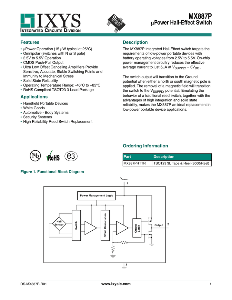
Figure 1. Functional Block Diagram
VSUPPLY
1
Output
Latch
Offset Cancellation
Hall
Sensor
Switch
Power Management Logic
Output
2
3
DS-MX887P-R01
www.ixysic.com
1
MX887P
INTEGRATED CIRCUITS DIVISION
1. Specifications . . . . . . . . . . . . . . . . . . . . . . . . . . . . . . . . . . . . . . . . . . . . . . . . . . . . . . . . . . . . . . . . . . . . . . . . . . . . . . . . . . . . . . . . . . . . . .
1.1 Package Pinout . . . . . . . . . . . . . . . . . . . . . . . . . . . . . . . . . . . . . . . . . . . . . . . . . . . . . . . . . . . . . . . . . . . . . . . . . . . . . . . . . . . . . . . . .
1.2 Pin Description. . . . . . . . . . . . . . . . . . . . . . . . . . . . . . . . . . . . . . . . . . . . . . . . . . . . . . . . . . . . . . . . . . . . . . . . . . . . . . . . . . . . . . . . . .
1.3 Absolute Maximum Ratings . . . . . . . . . . . . . . . . . . . . . . . . . . . . . . . . . . . . . . . . . . . . . . . . . . . . . . . . . . . . . . . . . . . . . . . . . . . . . . . .
1.4 Electrical Characteristics . . . . . . . . . . . . . . . . . . . . . . . . . . . . . . . . . . . . . . . . . . . . . . . . . . . . . . . . . . . . . . . . . . . . . . . . . . . . . . . . . .
1.5 ESD Rating . . . . . . . . . . . . . . . . . . . . . . . . . . . . . . . . . . . . . . . . . . . . . . . . . . . . . . . . . . . . . . . . . . . . . . . . . . . . . . . . . . . . . . . . . . . .
1.6 Magnetic Characteristics . . . . . . . . . . . . . . . . . . . . . . . . . . . . . . . . . . . . . . . . . . . . . . . . . . . . . . . . . . . . . . . . . . . . . . . . . . . . . . . . . .
3
3
3
3
3
4
4
2. Circuit Description. . . . . . . . . . . . . . . . . . . . . . . . . . . . . . . . . . . . . . . . . . . . . . . . . . . . . . . . . . . . . . . . . . . . . . . . . . . . . . . . . . . . . . . . . . . 4
3. Manufacturing Information . . . . . . . . . . . . . . . . . . . . . . . . . . . . . . . . . . . . . . . . . . . . . . . . . . . . . . . . . . . . . . . . . . . . . . . . . . . . . . . . . . . .
3.1 Moisture Sensitivity . . . . . . . . . . . . . . . . . . . . . . . . . . . . . . . . . . . . . . . . . . . . . . . . . . . . . . . . . . . . . . . . . . . . . . . . . . . . . . . . . . . . . .
3.2 ESD Sensitivity . . . . . . . . . . . . . . . . . . . . . . . . . . . . . . . . . . . . . . . . . . . . . . . . . . . . . . . . . . . . . . . . . . . . . . . . . . . . . . . . . . . . . . . . .
3.3 Reflow Profile. . . . . . . . . . . . . . . . . . . . . . . . . . . . . . . . . . . . . . . . . . . . . . . . . . . . . . . . . . . . . . . . . . . . . . . . . . . . . . . . . . . . . . . . . . .
3.4 Board Wash . . . . . . . . . . . . . . . . . . . . . . . . . . . . . . . . . . . . . . . . . . . . . . . . . . . . . . . . . . . . . . . . . . . . . . . . . . . . . . . . . . . . . . . . . . . .
3.5 Mechanical Dimensions. . . . . . . . . . . . . . . . . . . . . . . . . . . . . . . . . . . . . . . . . . . . . . . . . . . . . . . . . . . . . . . . . . . . . . . . . . . . . . . . . . .
2
www.ixysic.com
5
5
5
5
5
6
R01
MX887P
INTEGRATED CIRCUITS DIVISION
1 Specifications
1.1 Package Pinout
1.2 Pin Description
3
1
Pin#
Name
1
VSUPPLY
2
OUT
3
2
Description
2.5V to 5.5V
Push-Pull CMOS Output
GROUND Ground
1.3 Absolute Maximum Ratings
Parameter
Symbol
Min
Max
Units
Supply Voltage
VSUPPLY
-0.5
6
VDC
Output Voltage
VOUT
-0.5
6
V
-
Unlimited
5
G
mA
Junction Temperature
B
TJ
-
150
Operating Ambient Temperature
TA
-40
85
TSTG
-40
150
Magnetic Flux Density
Output Current
Storage Temperature
°C
Absolute maximum electrical ratings are at 25°C.
operation of the device at conditions beyond those
indicated in the operational sections of this data sheet
is not implied.
Absolute maximum ratings are stress ratings.
Stresses in excess of these ratings can cause
permanent damage to the device. Functional
1.4 Electrical Characteristics
Over operating voltage and temperature range unless otherwise specified.
Parameter
Conditions
Symbol
Minimum
Typical
Maximum
Units
Operating
VSUPPLY
2.5
-
5.5
VDC
VOUT=5.5V, BRPN < B < BRPS
ILKG
-
-
1
A
IOUT=1mA, VDD=3.0V
VOUT
-
100
300
mV
Awake Time
-
-
-
-
90
s
Period
-
-
-
-
90
ms
Duty Cycle
-
-
-
0.1
-
%
-
-
2
mA
-
-
8
A
-
5
15
A
Supply Voltage Range
Output Leakage Current
Output On Voltage
Supply Current
Awake (enabled)
Asleep (disabled)
ISUPPLY
Average (Calculated)
Notes:
R01
1. BOPX = operating point (output turns ON); BRPX = release point (output turns OFF).
2. Typical data is at 25°C and VSUPPLY = 3V.
www.ixysic.com
3
MX887P
INTEGRATED CIRCUITS DIVISION
1.5 ESD Rating
ESD Rating (Human Body Model)
2000V
1.6 Magnetic Characteristics
Over operating voltage and temperature range unless otherwise specified.
Parameter
Conditions
Symbol
Minimum
Typical
Maximum
Due to North Pole Applied
North Pole to Branded Side
BOPN
-60
-
-
Due to South Pole Applied
South Pole to Branded Side
BOPS
-
-
60
Due to North Pole Applied
North Pole to Branded Side
BRPN
-
-
-6
Due to South Pole Applied
South Pole to Branded Side
BRPS
6
-
-
| BOPX - BRPX |
BHYS
-
5
-
Units
Operating Points
G
Release Points
Hysteresis
Notes:
G
G
1. As used here, negative flux densities are defined as less than zero (algebraic convention); -50G<+10G.
2. BOPX = operating point (output turns ON); BRPX = release point (output turns OFF).
3. Typical data is at 25°C and VSUPPLY = 3V.
2 Circuit Description
The MX887P Power Hall-Effect Switch consists of a
Hall element, small-signal amplifier, latch, and CMOS
push-pull output. Offset cancellation circuitry rejects
errors in signal stages and the influence of mechanical
stress on the Hall element. This technique, together
with a precision threshold generator and comparator,
4
produces highly accurate magnetic switch points. The
Hall element is activated for a small fraction of an
operating cycle, then latched in that sample state for
the remainder of the period. By using this technique,
very low power consumption is achieved.
www.ixysic.com
R01
MX887P
INTEGRATED CIRCUITS DIVISION
3 Manufacturing Information
3.1 Moisture Sensitivity
All plastic encapsulated semiconductor packages are susceptible to moisture ingression. IXYS Integrated
Circuits Division classified all of its plastic encapsulated devices for moisture sensitivity according to the
latest version of the joint industry standard, IPC/JEDEC J-STD-020, in force at the time of product
evaluation. We test all of our products to the maximum conditions set forth in the standard, and guarantee
proper operation of our devices when handled according to the limitations and information in that standard as well as
to any limitations set forth in the information or standards referenced below.
Failure to adhere to the warnings or limitations as established by the listed specifications could result in reduced
product performance, reduction of operable life, and/or reduction of overall reliability.
This product carries a Moisture Sensitivity Level (MSL) rating as shown below, and should be handled according to
the requirements of the latest version of the joint industry standard IPC/JEDEC J-STD-033.
Device
Moisture Sensitivity Level (MSL) Rating
MX887P
MSL 3
3.2 ESD Sensitivity
This product is ESD Sensitive, and should be handled according to the industry standard
JESD-625.
3.3 Reflow Profile
This product has a maximum body temperature and time rating as shown below. All other guidelines of
J-STD-020 must be observed.
Device
Maximum Temperature x Time
MX887P
260°C for 30 seconds
3.4 Board Wash
IXYS Integrated Circuits Division recommends the use of no-clean flux formulations. However, board washing to
remove flux residue is acceptable, and the use of a short drying bake may be necessary. Chlorine-based or
Fluorine-based solvents or fluxes should not be used. Cleaning methods that employ ultrasonic energy should not be
used.
Pb
R01
e3
www.ixysic.com
5
MX887P
INTEGRATED CIRCUITS DIVISION
3.5 Mechanical Dimensions
3.5.1 MX887PHT TSOT23 3-Lead Package
Recommended PCB Land Pattern
0º / 8º
2.80 / 3.00
(0.110 / 0.118)
3
0.10 MIN
(0.004 MIN)
D
E1
E
2.60 / 3.00
(0.102 / 0.118)
1
0.00 / 0.10
(0.000 / 0.004)
1.05
(0.041)
0.10 / 0.25
(0.004 / 0.010)
0.60 REF
(0.0236 REF)
0.25 BSC
(0.0098 BSC)
5º NOM
7º NOM
0.95 BSC
(0.037 BSC)
0.60
(0.024)
0.95
(0.037)
GAUGE PLANE
0.70 / 0.80
(0.028 / 0.031)
2.70
(0.106)
2
0.35 / 0.51
(0.014 / 0.020)
0.75 / 0.90
(0.030 / 0.035)
0.37 / 0.47
(0.015 / 0.019)
1.50 / 1.70
(0.059 / 0.067)
1.90 BSC
(0.0748 BSC)
Dimensions
mm MIN / mm MAX
(inches MIN / inches MAX)
Notes: (Unless otherwise specified)
1. Dimension “D” does not include mold flash, protrusions, or gate burrs. Mold flash, protrusions, and gate burrs shall not exceed 0.10mm
(0.004 inches) per side.
2. Dimension “E” does not include inter-lead flash or protrusions. Inter-lead flash and protrusions shall not exceed 0.15mm (0.006 inches) per side.
3. Package top may be smaller than package bottom. Dimensions “D” and “E1” are determined at the outermost extreme of the plastic body
excluding mold flash, tie bar burrs, gate burrs, and interlead flash, but including any mismatch between top and bottom of the plastic body.
3.5.2 MX887PHTTR Tape & Reel Packaging
178 DIA.
(7.01 DIA.)
0.25 ± 0.05
(0.001 ± 0.002)
ø1.5, +0.1, -0
(ø0.059, +0.004, -0)
P=4.0 ± 0.1
(0.157 ± 0.004)
2.0 ± 0.05
(0.079 ± 0.002)
3.5 ± 0.05
(0.138 ± 0.002)
1.75 ± 0.1
(0.069 ± 0.004)
Top Cover
Tape Thickness
0.066 MAX.
(0.003 MAX.)
BO=3.2 ± 0.1
(0.126 ± 0.004)
K0=1.1 ± 0.1
(0.043 ± 0.004)
Embossed Carrier
Embossment
P=4.0 ± 0.1
(0.157 ± 0.004)
AO=3.2 ± 0.1
(0.126 ± 0.004)
ø1.1 ± 0.1
(0.043 ± 0.004)
W=8.0 ± 0.2
(0.315 ± 0.008)
Dimensions
mm
(inches)
NOTE: Tape dimensions not shown comply with JEDEC Standard EIA-481-2
For additional information please visit www.ixysic.com
IXYS Integrated Circuits Division makes no representations or warranties with respect to the accuracy or completeness of the contents of this publication and
reserves the right to make changes to specifications and product descriptions at any time without notice. Neither circuit patent licenses or indemnity are expressed
or implied. Except as set forth in IXYS Integrated Circuits Division’s Standard Terms and Conditions of Sale, IXYS Integrated Circuits Division assumes no liability
whatsoever, and disclaims any express or implied warranty relating to its products, including, but not limited to, the implied warranty of merchantability, fitness for a
particular purpose, or infringement of any intellectual property right.
The products described in this document are not designed, intended, authorized, or warranted for use as components in systems intended for surgical implant into
the body, or in other applications intended to support or sustain life, or where malfunction of IXYS Integrated Circuits Division’s product may result in direct physical
harm, injury, or death to a person or severe property or environmental damage. IXYS Integrated Circuits Division reserves the right to discontinue or make changes
to its products at any time without notice.
Specification: DS-MX887P-R01
©Copyright 2012, IXYS Integrated Circuits Division
All rights reserved. Printed in USA.
12/22/2012
6
www.ixysic.com
R01
