IDT5T9050
2.5V SINGLE DATA RATE 1:5 CLOCK BUFFER TERABUFFER JR.
INDUSTRIAL TEMPERATURE RANGE
2.5V SINGLE DATA RATE
1:5 CLOCK BUFFER
TERABUFFER™ JR.
IDT5T9050
NRND
NOT RECOMMENDED FOR NEW DESIGNS
DESCRIPTION:
FEATURES:
•
•
•
•
•
•
•
•
•
•
•
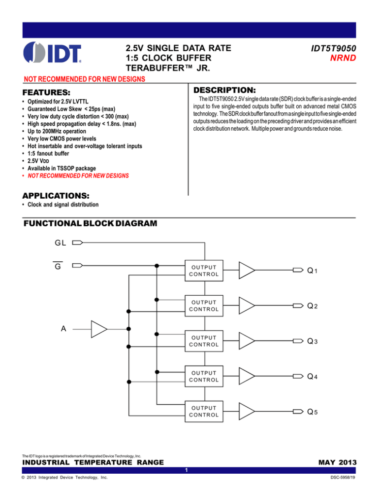
The IDT5T9050 2.5V single data rate (SDR) clock buffer is a single-ended
input to five single-ended outputs buffer built on advanced metal CMOS
technology. The SDR clock buffer fanout from a single input to five single-ended
outputs reduces the loading on the preceding driver and provides an efficient
clock distribution network. Multiple power and grounds reduce noise.
Optimized for 2.5V LVTTL
Guaranteed Low Skew < 25ps (max)
Very low duty cycle distortion < 300 (max)
High speed propagation delay < 1.8ns. (max)
Up to 200MHz operation
Very low CMOS power levels
Hot insertable and over-voltage tolerant inputs
1:5 fanout buffer
2.5V VDD
Available in TSSOP package
NOT RECOMMENDED FOR NEW DESIGNS
APPLICATIONS:
• Clock and signal distribution
FUNCTIONAL BLOCK DIAGRAM
GL
G
O U TPUT
C O N TR O L
Q1
O U TPUT
C O N TR O L
Q2
O U TPUT
C O N TR O L
Q3
O U TPUT
C O N TR O L
Q4
O U TPUT
C O N TR O L
Q5
A
The IDT logo is a registered trademark of Integrated Device Technology, Inc.
INDUSTRIAL TEMPERATURE RANGE
MAY 2013
1
© 2013 Integrated Device Technology, Inc.
DSC-5958/19
IDT5T9050
2.5V SINGLE DATA RATE 1:5 CLOCK BUFFER TERABUFFER JR.
INDUSTRIAL TEMPERATURE RANGE
PIN CONFIGURATION
ABSOLUTE MAXIMUM RATINGS(1)
Symbol
GL
1
28
GND
VDD
2
27
VDD
GND
3
26
GND
G
4
25
GND
V DD
5
24
VDD
Q1
6
23
Q2
GND
7
22
GND
A
8
21
Q3
Q5
9
20
Q4
V DD
10
19
VDD
GND
11
18
GND
VDD
12
17
GND
V DD
13
16
VDD
NC
14
15
NC
Description
Max
Unit
–0.5 to +3.6
V
Input Voltage
–0.5 to +3.6
V
Output Voltage
–0.5 to VDD +0.5
V
VDD
Power Supply Voltage
VI
VO
TSTG
Storage Temperature
–65 to +165
°C
TJ
Junction Temperature
150
°C
NOTE:
1. Stresses greater than those listed under ABSOLUTE MAXIMUM RATINGS may cause
permanent damage to the device. This is a stress rating only and functional operation
of the device at these or any other conditions above those indicated in the operational
sections of this specification is not implied. Exposure to absolute maximum rating
conditions for extended periods may affect reliability.
CAPACITANCE(1) (TA = +25°C, F = 1.0MHz)
Symbol
CIN
Parameter
Min
Typ.
Max.
Unit
Input Capacitance
—
6
—
pF
NOTE:
1. This parameter is measured at characterization but not tested.
TSSOP
TOP VIEW
RECOMMENDED OPERATING RANGE
Symbol
TA
VDD
Description
Ambient Operating Temperature
Internal Power Supply Voltage
Min.
–40
2.3
Typ.
+25
2.5
Max.
+85
2.7
Unit
°C
V
PIN DESCRIPTION
Symbol
A
G
I/O
I
I
Type
LVTTL
LVTTL
GL
Qn
VDD
I
O
LVTTL
LVTTL
PWR
Description
Clock input
Gate control for Qn outputs. When G is LOW, these outputs are enabled. When G is HIGH, these outputs are asynchronously
disabled to the level designated by GL(1).
Specifies output disable level. If HIGH, the outputs disable HIGH. If LOW, the outputs disable LOW.
Clock outputs
Power supply for the device core, inputs, and outputs
PWR
Power supply return for power
GND
NOTE:
1. Because the gate controls are asynchronous, runt pulses are possible. It is the user's responsibility to either time the gate control signals to minimize the possibility of runt
pulses or be able to tolerate them in down stream circuitry.
2
IDT5T9050
2.5V SINGLE DATA RATE 1:5 CLOCK BUFFER TERABUFFER JR.
INDUSTRIAL TEMPERATURE RANGE
DC ELECTRICAL CHARACTERISTICS OVER OPERATING RANGE(1)
Symbol
IIH
IIL
VIK
VIN
VIH
VIL
VOH
VOL
Parameter
Input HIGH Current
Input LOW Current
Clamp Diode Voltage
DC Input Voltage
DC Input HIGH(2)
DC Input LOW(3)
Output HIGH Voltage
Output LOW Voltage
Test Conditions
VDD = 2.7V
VI = VDD/GND
VDD = 2.7V
VI = GND/VDD
VDD = 2.3V, IIN = -18mA
IOH = -12mA
IOH = -100μA
IOL = 12mA
IOL = 100μA
Min.
—
—
—
- 0.3
1.7
—
VDD - 0.4
VDD - 0.1
—
—
Typ.(4)
—
—
- 0.7
Max
±5
±5
- 1.2
+3.6
—
0.7
—
—
0.4
0.1
Unit
μA
Typ.
1
Max
1.5
Unit
mA
100
150
μA/MHz
50
75
65
100
mA
V
V
V
V
V
V
V
V
NOTES:
1. See RECOMMENDED OPERATING RANGE table.
2. Voltage required to maintain a logic HIGH.
3. Voltage required to maintain a logic LOW.
4. Typical values are at VDD = 2.5V, +25°C ambient.
POWER SUPPLY CHARACTERISTICS
Symbol
IDDQ
IDDD
ITOT
Parameter
Quiescent VDD Power Supply Current
Dynamic VDD Power Supply
Current per Output
Total Power VDD Supply Current
Test Conditions(1)
VDD = Max., Reference Clock = LOW
Outputs enabled, All outputs unloaded
VDD = Max., CL = 0pF
VDD = 2.5V., FREFERENCE CLOCK = 100MHz, CL = 15pF
VDD = 2.5V., FREFERENCE CLOCK = 200MHz, CL = 15pF
NOTE:
1. The termination resistors are excluded from these measurements.
INPUT AC TEST CONDITIONS
Symbol
Parameter
Value
Units
VIH
Input HIGH Voltage
VDD
V
VIL
Input LOW Voltage
0
V
VTH
Input Timing Measurement Reference Level(1)
tR, tF
Input Signal Edge Rate(2)
VDD/2
V
2
V/ns
NOTES:
1. A nominal 1.25V timing measurement reference level is specified to allow constant, repeatable results in an automatic test equipment (ATE) environment.
2. The input signal edge rate of 2V/ns or greater is to be maintained in the 10% to 90% range of the input waveform.
3
IDT5T9050
2.5V SINGLE DATA RATE 1:5 CLOCK BUFFER TERABUFFER JR.
INDUSTRIAL TEMPERATURE RANGE
AC ELECTRICAL CHARACTERISTICS OVER OPERATING RANGE(4)
Symbol
Skew Parameters
Parameter
Min.
Typ.
Max
Unit
tSK(O)
Same Device Output Pin-to-Pin Skew(1)
—
—
25
ps
tSK(P)
Pulse Skew(2)
—
—
300
ps
Part-to-Part Skew(3)
—
—
300
ps
Propagation Delay A to Qn
—
—
1.8
ns
tSK(PP)
Propagation Delay
tPLH
tPHL
tR
Output Rise Time (20% to 80%)
350
—
850
ps
tF
Output Fall Time (20% to 80%)
350
—
850
ps
—
—
200
MHz
fO
Frequency Range
Output Gate Enable/Disable Delay
tPGE
Output Gate Enable to Qn
—
—
3.5
ns
tPGD
Output Gate Enable to Qn Driven to GL Designated Level
—
—
3
ns
NOTES:
1. Skew measured between all outputs under identical input and output transitions and load conditions on any one device.
2. Skew measured is the difference between propagation delay times tPHL and tPLH of any output under identical input and output transitions and load conditions on any one device.
3. Skew measured is the magnitude of the difference in propagation times between any outputs of two devices, given identical transitions and load conditions at identical VDD levels
and temperature.
4. Guaranteed by design.
AC TIMING WAVEFORMS
1/fo
tW
tW
V IH
V TH
A
V IL
tPHL
t PLH
V OH
V TH
Qn
V OL
t SK(O)
tSK(O)
V OH
V TH
Qm
V OL
Propagation and Skew Waveforms
NOTE: Pulse Skew is calculated using the following expression:
tSK(P) = | tPHL - tPLH |
where tPHL and tPLH are measured on the controlled edges of any one output from rising and falling edges of a single pulse. Please note that the tPHL and tPLH shown are not
valid measurements for this calculation because they are not taken from the same pulse.
4
IDT5T9050
2.5V SINGLE DATA RATE 1:5 CLOCK BUFFER TERABUFFER JR.
INDUSTRIAL TEMPERATURE RANGE
V IH
V TH
A
V IL
V IH
V TH
GL
V IL
t PLH
V IH
V TH
G
V IL
tPG E
t PGD
V OH
Qn
V TH
V OL
Gate Disable/Enable Showing Runt Pulse Generation
NOTE:
As shown, it is possible to generate runt pulses on gate disable and enable of the outputs. It is the user's responsibility to time their G signal to avoid this problem.
5
IDT5T9050
2.5V SINGLE DATA RATE 1:5 CLOCK BUFFER TERABUFFER JR.
INDUSTRIAL TEMPERATURE RANGE
TEST CIRCUIT AND CONDITIONS
V DD
V DD
V DD
R1
Pulse
Generator
V IN
R1
3 inch, ~50
Transmission Line
D.U.T.
A
Qn
R2
CL
Test Circuit for Input/Output
INPUT/OUTPUT TEST CONDITIONS
Symbol
VDD = 2.5V ± 0.2V
VTH
VDD / 2
V
R1
100
Ω
R2
100
Ω
CL
15
pF
6
Unit
R2
IDT5T9050
2.5V SINGLE DATA RATE 1:5 CLOCK BUFFER TERABUFFER JR.
INDUSTRIAL TEMPERATURE RANGE
ORDERING INFORMATION
IDT
XXXXX
Device Type
XX
X
Package Package
I
-40ºC to +85ºC (Industrial)
PGG
TSSOP - Green
5T9050
2.5V Single Data Rate 1:5 Clock Buffer
Terabuffer Jr.
7
IDT5T9050
2.5V SINGLE DATA RATE 1:5 CLOCK BUFFER TERABUFFER JR.
INDUSTRIAL TEMPERATURE RANGE
REVISION HISTORY
R ev
A
Table
P ag e
1
Discription of Change
Date
NRND - Not Recommended for New Designs
5/5/13
8
IDT5T9050
2.5V SINGLE DATA RATE 1:5 CLOCK BUFFER TERABUFFER JR.
INDUSTRIAL TEMPERATURE RANGE
We’ve Got Your Timing Solution.
6024 Silver Creek Valley Road
San Jose, CA 95138
Sales
Tech Support
800-345-7015 (inside USA)
+408-284-8200 (outside USA)
Fax: 408-284-2775
www.IDT.com/go/contactIDT
netcom@idt.com
+480-763-2056
DISCLAIMER Integrated Device Technology, Inc. (IDT) and its subsidiaries reserve the right to modify the products and/or specifications described herein at any time and at IDT’s sole discretion. All information
in this document, including descriptions of product features and performance, is subject to change without notice. Performance specifications and the operating parameters of the described products are determined
in the independent state and are not guaranteed to perform the same way when installed in customer products. The information contained herein is provided without representation or warranty of any kind, whether express
or implied, including, but not limited to, the suitability of IDT’s products for any particular purpose, an implied warranty of merchantability, or non-infringement of the intellectual property rights of others. This document
is presented only as a guide and does not convey any license under intellectual property rights of IDT or any third parties.
IDT’s products are not intended for use in applications involving extreme environmental conditions or in life support systems or similar devices where the failure or malfunction of an IDT product can be reasonably
expected to significantly affect the health or safety of users. Anyone using an IDT product in such a manner does so at their own risk, absent an express, written agreement by IDT.
Integrated Device Technology, IDT and the IDT logo are registered trademarks of IDT. Other trademarks and service marks used herein, including protected names, logos and designs, are the property of IDT or
their respective third party owners.
Copyright 2013. All rights reserved.
9
