QLx4270-DP
Features
The QLx4270-DP is a settable quad receive-side
equalizer with extended functionality for DisplayPort
applications. The QLx4270-DP compensates for the
frequency dependent attenuation of copper cables,
allowing operation on ultra-thin 40AWG cable.
• Supports data rates up to 2.7Gb/s per lane
• Low power (78mW per channel)
• Low latency (<500ps)
• Four equalizers in a 4mmx7mm QFN package for
straight route-through architecture and simplified
routing
The small form factor, highly-integrated quad design is
ideal for high-density data transmission applications
including active copper cable assemblies.
• Each equalizer boost is independently pin selectable
and programmable
Operating on a single 1.2V power supply, the
QLx4270-DP enables per channel throughputs of up to
2.7Gb/s. The QLx4270-DP uses current mode logic (CML)
inputs/outputs and is packaged in a 4mmx7mm 46 lead
QFN.
• 1.2V supply voltage
Applications
• DisplayPort (VESA DisplayPort Standard v1.1a)
• DisplayPort adaptors and repeaters
Benefits
• Thinner gauge cable
• Extends cable reach greater than 5x
• Improved BER
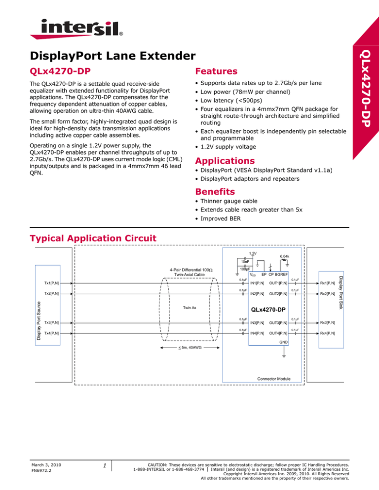
Typical Application Circuit
1.2V
6.04k
10nF
0.1µF
Tx1[P,N]
0.1µF
Tx2[P,N]
Display Port Source
100pF
VDD
Twin Ax
0.1µF
Tx4[P,N]
IN1[P,N]
IN2[P,N]
OUT1[P,N]
OUT2[P,N]
0.1µF
0.1µF
Rx1[P,N]
Rx2[P,N]
QLx4270-DP
0.1µF
Tx3[P,N]
EP CP BGREF
IN3[P,N]
IN4[P,N]
OUT3[P,N]
OUT4[P,N]
0.1µF
0.1µF
Display Port Sink
4-Pair Differential 100
Twin-Axial Cable
Rx3[P,N]
Rx4[P,N]
GND
< 5m, 40AWG
Connector Module
March 3, 2010
FN6972.2
1
CAUTION: These devices are sensitive to electrostatic discharge; follow proper IC Handling Procedures.
1-888-INTERSIL or 1-888-468-3774 | Intersil (and design) is a registered trademark of Intersil Americas Inc.
Copyright Intersil Americas Inc. 2009, 2010. All Rights Reserved
All other trademarks mentioned are the property of their respective owners.
QLx4270-DP
DisplayPort Lane Extender
QLx4270-DP
Ordering Information
PART NUMBER
(Note)
TEMP. RANGE
(°C)
PART MARKING
PACKAGE
(Pb-Free)
PKG. DWG. #
QLX4270RIQT7
QLX4270RIQ
0 to +70
46 Ld QFN
7” Prod. Tape & Reel; Qty 1,000
L46.4x7
QLX4270RIQSR
QLX4270RIQ
0 to +70
46 Ld QFN
7” Sample Reel; Qty 100
L46.4x7
NOTE: These Intersil Pb-free plastic packaged products employ special Pb-free material sets; molding compounds/die attach
materials and NiPdAu plate - e4 termination finish, which is RoHS compliant and compatible with both SnPb and Pb-free soldering
operations. Intersil Pb-free products are MSL classified at Pb-free peak reflow temperatures that meet or exceed the Pb-free
requirements of IPC/JEDEC J STD-020.
Pin Configuration
CP2[B]
CP2[C]
CP2[A]
CP1[B]
CP1[C]
CP1[A]
NC
NC
QLx4270-DP
(46 LD QFN)
TOP VIEW
46 45 44 43 42 41 40 39
DT
1
38 BGREF
IN1[P]
2
37 OUT1[P]
IN1[N]
3
36 OUT1[N]
VDD
4
35 VDD
IN2[P]
5
34 OUT2[P]
IN2[N] 6
33 OUT2[N]
VDD 7
32 VDD
EXPOSED PAD
(GND)
IN3[P] 8
31 OUT3[P]
IN3[N] 9
30 OUT3[N]
VDD 10
29 VDD
IN4[P] 11
28 OUT4[P]
IN4[N] 12
27 OUT4[N]
IS1 13
26 IS3
IS2 14
25 IS4
GND 15
24 GND
2
CP4[C]
CP4[B]
CP4[A]
CP3[C]
CP3[B]
CP3[A]
NC
NC
16 17 18 19 20 21 22 23
FN6972.2
March 3, 2010
QLx4270-DP
Pin Descriptions
PIN NAME
PIN
NUMBER
DT
1
IN1[P,N]
2, 3
Equalizer 1 differential input, CML. The use of 100nF low ESL/ESR MLCC capacitor with at least
4GHz frequency response is recommended.
VDD
4, 7, 10, 29,
32, 35
Power supply. 1.2V supply voltage. The use of parallel 100pF and 10nF decoupling capacitors to
ground is recommended for each of these pins for broad high-frequency noise suppression.
IN2[P,N]
5, 6
Equalizer 2 differential input, CML. The use of 100nF low ESL/ESR MLCC capacitor with at least
4GHz frequency response is recommended.
IN3[P,N]
8, 9
Equalizer 3 differential input, CML. The use of 100nF low ESL/ESR MLCC capacitor with at least
4GHz frequency response is recommended.
IN4[P,N]
11, 12
Equalizer 4 differential input, CML. The use of 100nF low ESL/ESR MLCC capacitor with at least
4GHz frequency response is recommended.
IS1
13
Impedance Select 1. CMOS logic input. When the voltage on this pin is LOW, the single-ended input
impedance of In1P and In1N each go above 200k and powers down the channel. This can be used
to disable some of the channels in case the DisplayPort application has less than four links, in order
to save power consumption. Otherwise, connect to VDD to hold the input impedance at 50.
IS2
14
Impedance Select 2. CMOS logic input. When the voltage on this pin is LOW, the single-ended input
impedance of In1P and In1N each go above 200k and powers down the channel. This can be used
to disable some of the channels in case the DisplayPort application has less than four links, in order
to save power consumption. Otherwise, connect to VDD to hold the input impedance at 50.
GND
15, 24
NC
16, 17, 45,
46
No-Connect
CP3[A,B,C]
18, 19, 20
Control pins for setting equalizer 3. CMOS logic inputs. Pins are read as a 3-digit number to set the
boost level. A is the MSB, and C is the LSB. Pins are internally pulled down through a 25k resistor.
CP4[A,B,C]
21, 22, 23
Control pins for setting equalizer 4. CMOS logic inputs. Pins are read as a 3-digit number to set the
boost level. A is the MSB, and C is the LSB. Pins are internally pulled down through a 25k resistor.
IS4
25
Impedance Select 4. CMOS logic input. When the voltage on this pin is LOW, the single-ended input
impedance of In1P and In1N each go above 200k and powers down the channel. This can be used
to disable some of the channels in case the DisplayPort application has less than four links, in order
to save power consumption. Otherwise, connect to VDD to hold the input impedance at 50.
IS3
26
Impedance Select 3. CMOS logic input. When the voltage on this pin is LOW, the single-ended input
impedance of In1P and In1N each go above 200k and powers down the channel. This can be used
to disable some of the channels in case the DisplayPort application has less than four links, in order
to save power consumption. Otherwise, connect to VDD to hold the input impedance at 50.
OUT4[N,P]
27, 28
Equalizer 4 differential output, CML. The use of 100nF low ESL/ESR MLCC capacitor with at least
4GHz frequency response is recommended.
OUT3[N,P]
30, 31
Equalizer 3 differential output, CML. The use of 100nF low ESL/ESR MLCC capacitor with at least
4GHz frequency response is recommended.
OUT2[N,P]
33, 34
Equalizer 2 differential output, CML. The use of 100nF low ESL/ESR MLCC capacitor with at least
4GHz frequency response is recommended.
OUT1[N,P]
36, 37
Equalizer 1 differential output, CML. The use of 100nF low ESL/ESR MLCC capacitor with at least
4GHz frequency response is recommended.
BGREF
38
CP2[C,B,A]
39, 40, 41
Control pins for setting equalizer 2. CMOS logic inputs. Pins are read as a 3-digit number to set the
boost level. A is the MSB, and C is the LSB. Pins are internally pulled down through a 25k resistor.
CP1[C,B,A]
42, 43, 44
Control pins for setting equalizer 1. CMOS logic inputs. Pins are read as a 3-digit number to set the
boost level. A is the MSB, and C is the LSB. Pins are internally pulled down through a 25k resistor.
Exposed Pad
-
Exposed ground pad. For proper electrical and thermal performance, this pad should be connected
to the PCB ground plane.
DESCRIPTION
Detection Threshold. Reference DC CURRENT threshold for input signal power detection. Data
output Out[k] is muted when the power of the equalized version of In[k] falls below the threshold.
Tie to ground to disable electrical idle preservation and always enable the limiting amplifier.
Ground
External bandgap reference resistor. Recommended value of 6.04kΩ ±1%.
3
FN6972.2
March 3, 2010
QLx4270-DP
Absolute Maximum Ratings
Thermal Information
Supply Voltage (VDD to GND) . . . . . . . . . . . . -0.3V to 1.3V
Voltage at All Input Pins . . . . . . . . . . . -0.3V to VDD + 0.3V
ESD Rating at all pins . . . . . . . . . . . . . . . . . . . . 2kV (HBM)
Thermal Resistance (Typical)
JA (°C/W) Jc (°C/W)
46 Ld QFN (Notes 1, 2) . . . . . . . . .
32
2.3
Operating Ambient Temperature Range . . . . . . 0°C to +70°C
Storage Ambient Temperature Range . . . . -55°C to +150°C
Maximum Junction Temperature . . . . . . . . . . . . . . . +125°C
Pb-Free Reflow Profile . . . . . . . . . . . . . . . . . .see link below
http://www.intersil.com/pbfree/Pb-FreeReflow.asp
CAUTION: Do not operate at or near the maximum ratings listed for extended periods of time. Exposure to such conditions may adversely impact
product reliability and result in failures not covered by warranty.
NOTES:
1. JA is measured with the component mounted on a high effective thermal conductivity test board in free air. See Tech Brief
TB379 for details.
2. For JC, the “case temp” location is the center of the exposed metal pad on the package underside.
Operating Conditions
PARAMETER
SYMBOL
Supply Voltage
Operating Ambient Temperature
MIN
TYP
MAX
UNITS
VDD
1.1
1.2
1.3
V
TA
0
25
70
°C
2.7
Gb/s
MAX
UNITS
NOTES
1
k
3
27.5
k
3
k
3
100
µA
Bit Rate
CONDITION
NRZ data applied to any channel
1.5
Control Pin Characteristics VDD = 1.2V, TA = +25°C, and VIN = 800mVP-P, unless otherwise noted.
PARAMETER
SYMBOL
CONDITION
MIN
‘LOW’ Resistance State
CP[k]
0
‘MID’ Resistance State
CP[k]
22.5
‘HIGH’ Resistance State
CP[k]
500
Input Current
Current draw on digital pin, i.e., CP[k]
TYP
25
30
NOTE:
3. If four CP pins are tied together, the resistance values in this table should be divided by four.
Electrical Characteristics VDD = 1.2V, TA = +25°C, and VIN = 800mVP-P, unless otherwise noted.
PARAMETER
SYMBOL
Supply Current
IDD
IC Input Amplitude
Range
VIN
CONDITION
MIN
TYP
MAX
260
Measured differentially at data source before
encountering channel loss
340
UNITS NOTES
mA
1380
mVP-P
DC Differential Input
Resistance
Measured on input channel IN[k]
80
100
120
DC Single-Ended Input
Resistance
Measured on input channel IN[k]P or IN[k]N
40
50
60
Input Return Loss
(Differential)
Output Amplitude Range
SDD11
VOUT
Differential Output
Impedance
50MHz to 1.35GHz
Measured differentially at OUT[k]P and OUT[k]N
with 50 load on both output pins
9
dB
4
5
150
550
650
mVP-P
Measured on OUT[k]
80
105
120
Output Return Loss
(Differential)
SDD22
50MHz to 1.35GHz
10
dB
5
Output Return Loss
(Common Mode)
SCC22
50MHz to 1.35GHz
5
dB
5
4
FN6972.2
March 3, 2010
QLx4270-DP
Electrical Characteristics VDD = 1.2V, TA = +25°C, and VIN = 800mVP-P, unless otherwise noted. (Continued)
PARAMETER
SYMBOL
SDC22
Output Return Loss
(Com. to Diff.
Conversion)
Output Residual Jitter
CONDITION
MIN
50MHz to 1.35GHz
tr, tf
MAX
20
2.7Gb/s; Up to 2m 38AWG standard twin-axial
cable (11.5dB loss)
Output Transition Time
TYP
20% to 80%
30
From IN[k] to OUT[k]
dB
5
0.15
0.2
UI
4, 6, 7
60
100
ps
8
50
ps
500
ps
Lane-to-Lane Skew
Propagation Delay
UNITS NOTES
NOTES:
4. After channel loss, differential amplitudes at QLx4270-DP inputs must meet the input voltage range specified in “Absolute
Maximum Ratings” on page 4.
5. Temperature = +25°C, VDD = 1.2V.
6. Output residual jitter is the difference between the total jitter at the lane extender output and the total jitter of the transmitted
signal (as measured at the input to the channel). Total jitter (TJ) is DJpp + 14.1 x RJRMS.
7. Measured using a PRBS 27-1 pattern. Deterministic jitter at the input to the lane extender is due to frequency-dependent,
media-induced loss only.
8. Rise and fall times measured using a 1GHz clock with a 20ps edge rate.
Control Pin Boost Setting
The voltages at the CP pins are used to determine the
boost level of each channel of QLx4270-DP. For each of
the four channels, k, the [A], [B], and [C] control pins
(CP[k]) are associated with a 3-bit non binary word.
While [A] can take one of two values, ‘LOW’ or ‘HIGH’,
[B] and [C] can take one of three different values: ‘LOW’,
‘MIDDLE’, or ‘HIGH’. This is achieved by changing the
value of a resistor connected between VDD and the CP
pin, which is internally pulled low with a 25k resistor.
Thus, a ‘HIGH’ state is achieved by using a 0 resistor,
‘MIDDLE’ is achieved with a 25k resistor, and ‘LOW’ is
achieved with an open resistance. Table 1 defines the
mapping from the 3-bit CP word to the 18 out of 32
possible levels available via the serial interface on the
Evaluation Board kit.
TABLE 1. MAPPING BETWEEN CP-SETTING RESISTOR
AND QLx4270-DP BOOST LEVELS
RESISTANCE BETWEEN CP PIN
AND VDD
CP[A]
CP[B]
CP[C]
SERIAL BOOST
LEVEL
Open
Open
Open
0
Open
Open
25k
2
Open
Open
0
4
Open
25k
Open
6
Open
25k
25k
8
Open
25k
0
10
Open
0
Open
12
Open
0
25k
14
Open
0
0
15
0
Open
Open
16
5
TABLE 1. MAPPING BETWEEN CP-SETTING RESISTOR
AND QLx4270-DP BOOST LEVELS (Continued)
RESISTANCE BETWEEN CP PIN
AND VDD
CP[A]
CP[B]
CP[C]
SERIAL BOOST
LEVEL
0
Open
25k
17
0
Open
0
19
0
25k
Open
21
0
25k
25k
23
0
25k
0
24
0
0
Open
26
0
0
25k
28
0
0
0
31
If all four channels are to use the same boost level, then
a minimum number of board resistors can be realized by
tying together like CP[k][A,B,C] pins across all channels
k. For instance, all four CP[k][A] pins can be tied to the
same resistor running to VDD. Consequently, only three
resistors are needed to control the boost of all four
channels. If the CP Pins are tied together and the 25k is
used, the value changes to a 3.125k resistor because
the 25k is divided by 4.
Channel Power-Down
The IS[k] pin powers down the equalizer channel when
pulled low. This feature allows individually to power down
unused channels and to minimize power consumption.
Example: for DisplayPort applications with 1 or 2 links,
the unused channels may be powered down to save
power. The current draw for a channel is reduced from
50mA to 3.8mA when powered down.
FN6972.2
March 3, 2010
QLx4270-DP
About Q:Active®
Historically, cable manufacturers have relied on
thick wire gauge cables to deliver Deep Color
images to the monitors and projectors. However,
these cables are bulky, unwieldy and esthetically
unappealing. To address this, Intersil has
developed its groundbreaking Q:ACTIVE® product
line. By integrating its analog ICs inside DisplayPort
cables, Intersil is able to achieve unsurpassed
improvements in cable gauges, reach and
transmitted image quality.
For additional products, see www.intersil.com/product_tree
Intersil products are manufactured, assembled and tested utilizing ISO9000 quality systems as noted
in the quality certifications found at www.intersil.com/design/quality
Intersil products are sold by description only. Intersil Corporation reserves the right to make changes in circuit design, software and/or specifications
at any time without notice. Accordingly, the reader is cautioned to verify that data sheets are current before placing orders. Information furnished by
Intersil is believed to be accurate and reliable. However, no responsibility is assumed by Intersil or its subsidiaries for its use; nor for any
infringements of patents or other rights of third parties which may result from its use. No license is granted by implication or otherwise under any
patent or patent rights of Intersil or its subsidiaries.
For information regarding Intersil Corporation and its products, see www.intersil.com
6
FN6972.2
March 3, 2010
QLx4270-DP
Package Outline Drawing
L46.4x7
46 LEAD THIN QUAD FLAT NO-LEAD PLASTIC PACKAGE (TQFN)
Rev 0, 9/09
2.80
4.00
42X 0.40
A
B
6
PIN 1
INDEX AREA
38
7.00
(4X)
46
39
6
PIN 1
INDEX AREA
1
5.50 ±0.1
Exp. DAP
5.60
15
24
0.05
46X 0.20 4
0.10 M C A B
SIDE VIEW
TOP VIEW
16
23
2.50 ±0.1
Exp. DAP
46X 0.40
BOTTOM VIEW
SEE DETAIL "X"
0.10 C
0.70 ±0.05
C
SEATING PLANE
0.05 C
SIDE VIEW
C
0.152 REF
5
0 . 00 MIN.
0 . 05 MAX.
DETAIL "X"
( 3.80 )
( 2.50)
NOTES:
( 6.80 )
( 42X 0.40)
( 5.50 )
1.
Dimensions are in millimeters.
Dimensions in ( ) for Reference Only.
2.
Dimensioning and tolerancing conform to AMSE Y14.5m-1994.
3.
Unless otherwise specified, tolerance : Decimal ± 0.05
4.
Dimension applies to the metallized terminal and is measured
between 0.15mm and 0.30mm from the terminal tip.
(46X 0.20)
5.
Tiebar shown (if present) is a non-functional feature.
6.
The configuration of the pin #1 identifier is optional, but must be
located within the zone indicated. The pin #1 identifier may be
either a mold or mark feature.
( 46 X 0.60)
TYPICAL RECOMMENDED LAND PATTERN
7
FN6972.2
March 3, 2010


