NXP Load
Switches and
Over-Voltage
Protection ICs
Simple, efficient, protection and control
with smallest footprint
NXP’s integrated load switch and OVP families, NX3P/NX5P/NX18P, provide simple
and efficient power distribution solutions to reduce system power consumption,
while providing robust protection against voltage and current surges. Designed in
the smallest packages to address mobile and portable applications, they greatly
reduce design complexity and time to market.
KEY FEATURES
BENEFITS
• Low ON resistance for highest efficiency
• In-rush current control
• Over-voltage tolerant inputs to 30 V
• Over-voltage protection (OVP)
• Over-current protection (OCP)
• Over-temperature protection (OTP)
• Reverse current protection (RCP)
• Output discharge circuit to remove capacitive load
• Integrated 8 kV IEC6100-4-2 (contact) ESD diodes
• Protects from over-voltage, over-current surges
• Extends battery life by disconnecting unused sub-systems
• Replace multiple discretes and LDOs lowering total part
count
Applications
OVP and OCP functions safeguard PMIC and sub-blocks
from poorly regulated supplies during charge, and from
faulty loads while in OTG mode.
•Smart phones/tablet PC’s/notebooks
•Digital cameras
•Portable medical devices
•Other power sensitive applications
With very low leakage current, and low ON resistance,
NX3P/NX5P/NX18P high-side load switches are ideal to
manage power distribution to sub-systems while reducing
total power dissipation.
Available in extremely small plastic and WLCSP packages,
they can provide a continuous current from 200 mA to 3.0 A
while operating from -40 to 85ºC.
Protection and control
Packages
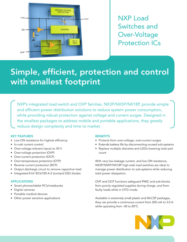
NXP’s load switches integrate reverse-current/voltage
protection, over-voltage protection, over-current protection
and over-temperature protection, actively protecting it and
the components it supplies, when a system-fail event is
detected.
Built in small footprint SOT, leadless QFN, and WLCSP
packages,these load switches also integrate ESD IEC610004-2 protection making them ideal for portable applications
where board space is at a premium. Requiring minimal
external components, the low-pin count further improves
crowded layouts, by simplifying routing and eliminate
dependencies of intricate line-layout patterns.
Integrated slew-rate control reduces inrush current
associated with system start-up, while the ILIM-feature
limits the maximum switch current.
NXP packages are Dark Green, Pb-free, RoHS compliant.
Equipped with a low-threshold logic enable input, it can be
used with both new and legacy controllers.
For more information about NXP load switches visit:
www.nxp.com/products/logic/load_switches
Under-voltage and over-voltage lock-out ensure the switch
remains disabled until issues are removed before resuming
normal operation.
NX LOAD SWITCH PORTFOLIO
Device
Target Applications
VIN (V)
RON
(mΩ)
IMAX
(A)
ILIM
Slew
rate
Rdch
OCP
RCP
UVLO OVLO
OTP
Package
NX3P190
Mobile computing
1.1 – 3.6
65
0.5
•
NX3P191
Mobile computing
1.1 – 3.6
65
0.5
•
•
WLCSP-4
•
WLCSP-4
NX3P2902B
Mobile computing
1.1 – 3.6
65
0.5
•
NX3P1107
Mobile computing
0.9 – 3.6
35
1.5
•
WLCSP-4
WLCSP-4(a)
NX3P1108
Mobile computing
0.9 – 3.6
35
1.5
•
•
WLCSP-4(a)
NX5P2924
Mobile computing
1.0 – 5.5
18
2.5
•
•
WLCSP-6
NX5P1000
USB-OTG
3.0 – 5.5
60
1
•
•
NX5P2553
TV, LCD, DSC
2.5 – 6.5
60
1.7
•
•
NX5P2090
USB-OTG, smart phone 3.0 – 5.5
60
2
•
•
•
•
•
•
•
•
•
•
•
WLCSP-12
•
SOT457,
SOT1348-1
WLCSP-9
NX5P3001
Tablet, hard drive
3.2 – 6.35
62
3
•
•
•
•
WLCSP-12
NX18P3001
Smart phone, tablet
3.2 – 17.5
62
3
•
•
•
•
WLCSP-12
Package Pins
suffix
Package
Outline Width Length Height Pitch
(mm) (mm)
(mm) (mm)
Package Pins
suffix
Package
Outline Width Length Height Pitch
(mm) (mm)
(mm) (mm)
UK
4
WLCSP-4
0.76
0.76
0.51
0.40
UK
6
WLCSP-6
0.87
1.37
0.50
0.50
UK
4
WLCSP-4(a)
0.96
0.96
0.55
0.50
UK
9
WLCSP-9
1.36
1.36
0.51
0.40
GV
6
SOT457
1.50
2.90
1.00
0.95
UK
12
WLCSP-12
1.36
1.66
0.51
0.40
GU
6
SOT1348-1
2.00
2.00
0.50
0.65
www.nxp.com
© 2013 NXP Semiconductors, B.V.
All rights reserved. Reproduction in whole or in part is prohibited without the prior written consent of the copyright owner. The informa-
Date of release: Month 2013
tion presented in this document does not form part of any quotation or contract, is believed to be accurate and reliable and may be
Document order number: 9397 750 17475
changed without notice. No liability will be accepted by the publisher for any consequence of its use. Publication thereof does not convey
Published in the USA
nor imply any license under patent or other industrial or intellectual property rights.
