Supertex inc.
DN2625
N-Channel Depletion-Mode Vertical DMOS
FET in Single and Dual Options
Features
General Description
►
►
►
►
►
►
The Supertex DN2625 is a low threshold depletion-mode
(normally-on) transistor utilizing an advanced vertical DMOS
structure and Supertex’s well-proven silicon-gate manufacturing
process. This combination produces a device with the power
handling capabilities of bipolar transistors and with the high
input impedance and positive temperature coefficient inherent in
MOS devices. Characteristic of all MOS structures, this device
is free from thermal runaway and thermally-induced secondary
breakdown.
Very low gate threshold voltage
Designed to be source-driven
Low switching losses
Low effective output capacitance
Designed for inductive loads
Well matched for low second harmonic when
driven by Supertex MD2130
Applications
►
►
►
►
►
►
►
►
Medical ultrasound beamforming
Ultrasonic array focusing transmitter
Piezoelectric transducer waveform drivers
High speed arbitrary waveform generator
Normally-on switches
Solid state relays
Constant current sources
Power supply circuits
Supertex’s vertical DMOS FETs are ideally suited to a wide range
of switching and amplifying applications where high breakdown
voltage, high input impedance, low input capacitance, and fast
switching speeds are desired.
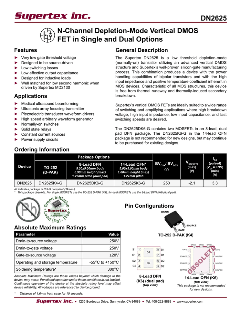
The DN2625DK6-G contains two MOSFETs in an 8-lead, dual
pad DFN package. The DN2625K6-G in the 14-lead QFN
package is not recommended for new designs, but may continue
to be purchased for existing designs.
Ordering Information
Package Options
8-Lead DFN
14-Lead QFN*
Device
TO-252
(D-PAK)
5.00x5.00mm body
0.90mm height (max)
1.27mm pitch (dual pad)
5.00x5.00mm body
1.00mm height (max)
1.27mm pitch
DN2625
DN2625K4-G
DN2625DK6-G
DN2625K6-G
IDS
VGS(OFF)
BVDSX/ BVDGX
(V)
(max)
(V)
(pulsed)
(VGS = 0.9V)
(min)
(A)
250
-2.1
3.3
-G indicates package is RoHS compliant (‘Green’)
* This package obsolete. For single MOSFETs use the TO-252 D-PAK (K4), for dual MOSFETs use the 8-Lead DFN (K6) (dual pad).
Pin Configurations
DRAIN
Absolute Maximum Ratings
SOURCE
Parameter
Value
Drain-to-source voltage
250V
Drain-to-gate voltage
250V
S1
1
Gate-to-source voltage
±20V
G1
2
-55 C to +150 C
S2
3
300OC
Absolute Maximum Ratings are those values beyond which damage to the
device may occur. Functional operation under these conditions is not implied.
Continuous operation of the device at the absolute rating level may affect
device reliability. All voltages are referenced to device ground.
Distance of 1.6mm from case for 10 seconds.
Supertex inc.
G2 4
D2
7 D1
6 D2
5 D2
SOURCE 2
SOURCE 3
SOURCE 4
8-Lead DFN
(K6) (dual pad)
(top view)
12
E
1
DRAIN
T
8 D1
13
LE
D1
DRAIN
14
O
O
DRAIN
GATE
B
S
Soldering temperature*
O
TO-252 D-PAK (K4)
O
Operating and storage temperature
*
GATE
5
DRAIN
6
DRAIN
11 GATE
10 SOURCE
9 SOURCE
7
8 SOURCE
DRAIN
14-Lead QFN (K6)
(top view)
This package is not recommended
for new designs.
● 1235 Bordeaux Drive, Sunnyvale, CA 94089 ● Tel: 408-222-8888 ● www.supertex.com
DN2625
Product Marking
TO-252 D-PAK (K4)
8-Lead DFN (K6) (dual pad)
Thermal Characteristics
ID
ID
T
L = Lot Number
YY = Year Sealed
WW = Week Sealed
A = Assembler ID
C = Country of Origin
= “Green” Packaging
O
LE
DN2625
LLLLLL
YYWW
AAACCC
S
YY = Year Sealed
WW = Week Sealed
L = Lot Number
= “Green” Packaging
L = Lot Number
YY = Year Sealed
WW = Week Sealed
A = Assembler ID
C = Country of Origin
= “Green” Packaging
O
B
Si YYWW
DN2625
LLLLLLL
D2625D
LLLLLL
YYWW
AAACCC
E
Packages may or may not include the following marks: Si or
14-Lead QFN (K6)
This package is not recommended
for new designs.
Package
(continuous)1
(A)
(pulsed)
(A)
Rθja
Rθjc
IDR1
IDRM
( C/W)
( C/W)
(A)
(A)
D-PAK
1.1
3.3
502
5.5
1.1
3.3
8-Lead DFN (dual pad)
1.1
3.3
32
3
3.2
1.1
3.3
14-Lead QFN
1.1
3.3
22
3
2.0
1.1
3.3
O
O
4
Notes:
1. ID (Continuous) is limited by max. Tj.
2. 4-layer, 1oz, 3x4inch PCB, with 20-via for drain pad.
3. 4-layer, 1oz, 3x4inch PCB, with 12-via for drain pad.
4. Junction to the DFN thermal pad.
Electrical Characteristics (T
A
= 25OC unless otherwise specified)
Sym
Parameter
Min
Typ
Max
Units
BVDSX
Drain-to-source breakdown voltage
250
-
-
V
VGS = -2.5V, ID = 50µA
BVDGX
Drain-to-gate breakdown voltage
250
-
-
V
VGS = -2.5V, ID = 50µA
VGS(OFF)
Gate-to-source off voltage
-1.5
-
-2.1
V
VDS = 15V, ID = 100µA
Change in VGS(OFF) with temperature
-
-
-4.5
mV/ C
VDS = 15V, ID = 100µA
Gate body leakage current
-
-
100
nA
VGS = ±20V, VDS = 0V
-
-
1.0
-
-
200
Saturated drain-to-source current
1.1
-
-
A
VGS = 0V, VDS = 15V
IDS(PULSE)
Pulsed drain-to-source current
3.1
3.3
-
A
VGS = 0.9V, VDS = 15V
(with duty cycle of 1%)
RDS(ON)
Static drain-to-source on-resistance
-
-
3.5
Ω
VGS = 0V, ID = 1.0A
ΔRDS(ON)
Change in RDS(ON) with temperature
-
-
1.1
%/ C
VGS = 0V, ID = 200mA
100
-
-
mmho
VDS = 10V, ID = 150mA
ΔVGS(OFF)
IGSS
ID(OFF)
IDSS
Drain-to-source leakage current
GFS
Forward transconductance
CISS
Input capacitance
-
800
1000
COSS
Common source output capacitance
-
70
210
CRSS
Reverse transfer capacitance
-
18
70
td(ON)
Turn-on delay time
-
-
10
Rise time
-
-
20
Turn-off delay time
-
-
10
tr
td(OFF)
Fall time
-
-
20
VSD
tf
Diode forward voltage drop
-
-
1.8
QG
Total gate charge
-
-
7.04
QGS
Gate-to-source charge
-
-
0.783
QGD
Gate-to-drain charge
-
-
3.73
Supertex inc.
O
µA
O
Conditions
VDS = 250V, VGS = -5.0V
VDS = 250V, VGS = -5.0V, TA = 125OC
pF
VGS = -2.5V,
VDS = 25V,
f = 1.0MHz
ns
VDD = 25V,
ID = 150mA,
RGEN = 3.0Ω,
VGS = 0v to -10V
V
VGS = -2.5V, ISD = 150mA
nC
ID = 3.5A,
VDS = 100V,
VGS = 1.5V
● 1235 Bordeaux Drive, Sunnyvale, CA 94089 ● Tel: 408-222-8888 ● www.supertex.com
2
DN2625
Switching Waveforms and Test Circuit
0V
VDD
90%
INPUT
-10V
RL
Pulse
Generator
10%
t(ON)
t(OFF)
td(ON)
VDD
RGEN
td(OFF)
tr
tf
0V
INPUT
10%
10%
OUTPUT
OUTPUT
90%
D.U.T.
90%
Typical Performance Curves
Saturation Characteristics
Output Characteristics
5.5
7.0
VGS = -1.5V
VGS = -1V
4.5
6.0
VGS = 1.5V
VGS = 0V
VGS = 0.5V
3.5
VGS = 1.0V
VGS = 0.5V
4.0
VGS = -0.5V
4.0
VGS = 2.0V
5.0
ID (A)
ID (amps)
VGS = -2V
5.0
VGS = 0V
VGS = -0.5V
3.0
VGS = -1.0V
2.0
VGS = -2.0V
VGS = 1V
VGS = 1.5V
3.0
VGS = 2V
2.5
2.0
VGS = -1.5V
1.5
1.0
1.0
0.5
0.0
0
50
100
150
200
VDS (volts)
0.0
250
0
1
2
3
4
5
VDS (V)
6
7
8
9
10
BVDSX Variation With Temperature
Transfer Characteristics
10
-55OC
9
1.20
1.15
ID (amps)
7
25OC
6
125OC
5
4
3
2
1.10
1.05
VGS = -2.5V
ID = 1mA
1.00
0.95
0.90
0.85
1
0
BVDSX (normalized)
8
-3.0
-2.0
-1.0
0.0
1.0
VGS (V)
Supertex inc.
2.0
3.0
4.0
0.80
-50
-25
0
25
50
75
100
Tj (OC)
● 1235 Bordeaux Drive, Sunnyvale, CA 94089 ● Tel: 408-222-8888 ● www.supertex.com
3
125
150
DN2625
Typical Performance Curves (cont.)
Transconductance vs Drain Current
On-Resistance vs Drain Current
5.0
4.0
VGS = 1V
4.5
3.5
4.0
GFS (Siemens)
RDS(ON) (ohms)
-55OC
3.0
3.5
3.0
2.5
2.0
1.5
1.0
2.5
25OC
2.0
1.5
1.0
125OC
0.5
0.5
0.0
VDS = 10V
0.0
0.5
1.0
1.5
2.0
2.5
3.0
3.5
4.0
4.5
5.0
5.5
0.0
0.0
0.5
1.0
1.5
2.0
2.5
3.0
3.5
4.0
4.5
ID (A)
ID (A)
1.25
2.50
1.20
2.25
1.15
2.00
1.75
1.10
VGS(OFF) @100µA
VDS = 15V
1.05
1.50
1.25
1.00
0.95
1.00
RDS(ON) @VGS = 1V
ID =1A
0.90
0.75
0.50
0.85
0.80
RDS(ON) (normalized)
VGS(OFF) (normalized)
VGS(OFF) and RDS(ON) Variation With Temperature
-50
-25
0
25
50
75
100
125
0.25
150
Tj (OC)
Supertex inc.
● 1235 Bordeaux Drive, Sunnyvale, CA 94089 ● Tel: 408-222-8888 ● www.supertex.com
4
5.0
5.5
6.0
DN2625
3-Lead TO-252 D-PAK Package Outline (K4)
b3
E
A
c2
E1
4
L3
θ1
D1
H
D
1
2
3
L4
L5
Note 1
b2
Front View
View B
b
e
Side View
Rear View
Gauge
Plane
A1
Seating
Plane
L2
θ
L
L1
View B
Note:
1. Although 4 terminal locations are shown, only 3 are functional. Lead number 2 was removed.
Symbol
Dimension
(inches)
MIN
A
A1
b
b2
b3
c2
D
D1
E
E1
.086
.000*
.025
.030
.195
.018
.235
.205
.250
.170
NOM
-
-
-
-
-
-
.240
-
-
-
MAX
.094
.005
.035
.045
.215
.035
.245
.217*
.265
.182*
e
.090
BSC
H
L
.370
.055
-
.060
.410
.070
L1
L2
.108
REF
.020
BSC
L3
L4
L5
θ
θ1
.035
.025*
.045
0O
0O
-
-
-
-
-
.050
.040
.060
10O
15O
JEDEC Registration TO-252, Variation AA, Issue E, June 2004.
* This dimension is not specified in the JEDEC drawing.
Drawings not to scale.
Supertex Doc. #: DSPD-3TO252K4, Version E041309.
Supertex inc.
● 1235 Bordeaux Drive, Sunnyvale, CA 94089 ● Tel: 408-222-8888 ● www.supertex.com
5
DN2625
8-Lead DFN Package Outline (K6)
5.00x5.00mm body, 0.90mm height (max), 1.27mm pitch (dual pad)
K1
D
8
D2
K1/2
D2
8
E2
E
E2
Note 1
Note 1
(Index Area
D/2 x E/2)
Note 1
(Index Area
D/2 x E/2)
1
1
Top View
Bottom View
View B
Note 3
θ
A
A3
e
b
A1
L
Seating
Plane
L1
Note 2
View B
Side View
Notes:
1. A Pin 1 identifier must be located in the index area indicated. The Pin 1 identifier can be: a molded mark/identifier; an embedded metal marker; or
a printed indicator.
2. Depending on the method of manufacturing, a maximum of 0.15mm pullback (L1) may be present.
3. The inner tip of the lead may be either rounded or square.
Symbol
Dimension
(mm)
A
A1
MIN
0.80
0.00
NOM
0.85
-
MAX
0.90
0.05
A3
0.20
REF
b
D
D2
E
E2
0.35
4.90
1.93
4.90
1.90
0.40
5.00
2.03
5.00
2.00
0.45
5.10
2.13
5.10
2.10
e
1.27
BSC
K1
0.40
REF
L
L1
θ
0.40
0.00
0O
0.50
-
-
0.60
0.15
14O
Drawings not to scale
Supertex Doc. #: DSPD-8DFNK65x5P127, Version A040209
Supertex inc.
● 1235 Bordeaux Drive, Sunnyvale, CA 94089 ● Tel: 408-222-8888 ● www.supertex.com
6
DN2625
14-Lead QFN Package Outline (K6)
5.00x5.00mm body, 1.00mm height (max), 1.27mm pitch
E2
E
14
14
Pin 1
E
1
T
Note 1
(Index Area
D/2 x E/2)
D2
LE
D
O
Top View
S
Exposed
Pad
e
DD
BB
Bottom View
CC
Seating
Plane
B
A3
Note 1
(Index Area
D/2 x E/2)
b
AA
θ
A
e
A1
O
Side View
Notes:
1. A Pin 1 identifier must be located in the index area indicated. The Pin 1 identifier can be: a molded mark/identifier; an embedded metal marker; or
a printed indicator.
Symbol
A
A1
MIN
Dimension
NOM
(mm)
MAX
0.80
0.00
0.90
0.02
1.00
0.05
A3
0.20
REF
b
D
D2
E
E2
0.46
4.85
4.45
4.85
2.52
0.51
5.00
4.50
5.00
2.57
0.58
5.15
4.55
5.15
2.62
e
1.27
BSC
AA
BB
CC
DD
θ
0.152 0.473
0.66 0.456
0O
0.252 0.523
0.71 0.506
-
0.352 0.583
0.77 0.566 14O
Drawings not to scale.
Supertex Doc. #: DSPD-14QFNK65X5P127, Version B090808.
(The package drawing(s) in this data sheet may not reflect the most current specifications. For the latest package outline
information go to http://www.supertex.com/packaging.html.)
Supertex inc. does not recommend the use of its products in life support applications, and will not knowingly sell them for use in such applications unless it receives
an adequate “product liability indemnification insurance agreement.” Supertex inc. does not assume responsibility for use of devices described, and limits its liability
to the replacement of the devices determined defective due to workmanship. No responsibility is assumed for possible omissions and inaccuracies. Circuitry and
specifications are subject to change without notice. For the latest product specifications refer to the Supertex inc. (website: http//www.supertex.com)
Supertex inc.
©2010 Supertex inc. All rights reserved. Unauthorized use or reproduction is prohibited.
Doc.# DSFP-DN2625
B052110
1235 Bordeaux Drive, Sunnyvale, CA 94089
Tel: 408-222-8888
www.supertex.com
7


