GO1525 HD-LINX™II
Voltage Controlled Oscillator
GO1525 Data Sheet
Key Features
•
generates 1.485GHz or 1.485/1.001GHz signal for
HD-LINX™II ICs
•
low current consumption
•
50Ω output impedance
•
operates from a single 2.5V supply
•
8 pin tape on reel
•
Pb-free and RoHS Compliant
The output level is typically -9.0dBm with low spurious
and noise content. It is designed to drive 50Ω strip lines.
VCO for the GS1560, GS1559 and GS9060
Deserializers, and the GS1532, GS1531 and
GS9062 Serializers
This component and all homogeneous subcomponents
are RoHS compliant.
Description
GO1555 for new designs
The GO1525 is a self contained, miniature Voltage
Controlled Oscillator (VCO). It produces a clean
1.485GHz reference clock signal for the GS1560 and
GS9060 deserializers, and for the GS1532 and
The GO1555 should be used for new designs given that
it is smaller, consumes less power and gives better jitter
performance.
VCTR
VCC
STRIPLINE
STRIPLINE
OUT
OSCILLATOR CIRCUIT
GND
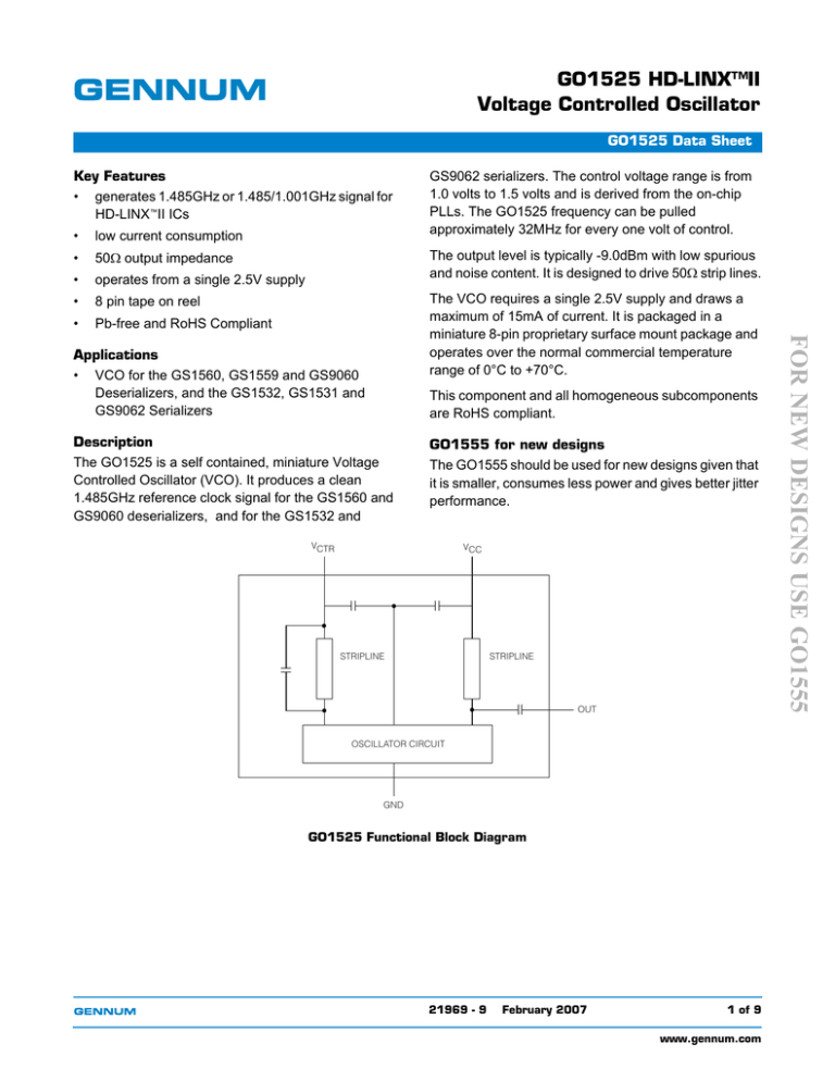
GO1525 Functional Block Diagram
21969 - 9
February 2007
1 of 9
www.gennum.com
FOR NEW DESIGNS USE GO1555
The VCO requires a single 2.5V supply and draws a
maximum of 15mA of current. It is packaged in a
miniature 8-pin proprietary surface mount package and
operates over the normal commercial temperature
range of 0°C to +70°C.
Applications
•
GS9062 serializers. The control voltage range is from
1.0 volts to 1.5 volts and is derived from the on-chip
PLLs. The GO1525 frequency can be pulled
approximately 32MHz for every one volt of control.
GO1525 Data Sheet
Contents
Key Features .................................................................................................................1
Applications...................................................................................................................1
Description ....................................................................................................................1
1. Pin Out ......................................................................................................................3
1.1 Pin Assignment ...............................................................................................3
1.2 Pin Descriptions ..............................................................................................3
2. Electrical Characteristics ...........................................................................................4
3.1 Reflow Conditions ...........................................................................................6
3.2 Soldering Flux .................................................................................................6
3.3 Rework or Repair ............................................................................................6
3.4 Endurance To Warp ........................................................................................6
4. Handling Recommendations .....................................................................................7
4.1 Cleaning ..........................................................................................................7
4.2 Storage ...........................................................................................................7
4.3 Transport .........................................................................................................7
4.4 ESD Warning ..................................................................................................7
5. Package & Ordering Information ...............................................................................8
5.1 Package Dimensions ......................................................................................8
5.2 Packaging Data ...............................................................................................8
5.3 Ordering Information .......................................................................................8
6. Revision History ........................................................................................................9
21969 - 9
February 2007
2 of 9
FOR NEW DESIGNS USE GO1555
3. Soldering Recommendations ....................................................................................5
GO1525 Data Sheet
1. Pin Out
1.1 Pin Assignment
GND
NC
GND
O/P
3
2
1
GO1525
4
8
GND
TOP VIEW
6
7
VCTR
GND
VCC
FOR NEW DESIGNS USE GO1555
5
NOTE: Pin numbers are arbitrary
There are no pin markings on the device itself
1.2 Pin Descriptions
Table 1-1: Pin Descriptions
Pin Number
Name
Type
Description
2, 4, 6, 8
GND
Power
Most negative power supply connections.
5
VCTR
Input
Control voltage for the VCO.
7
VCC
Power
Most positive power supply connection.
1
O/P
Output
VCO signal output.
3
NC
–
No connection.
Note: Pin numbering different from GO1515
21969 - 9
February 2007
3 of 9
GO1525 Data Sheet
2. Electrical Characteristics
Table 2-1: Electrical Characteristics
VCC = 2.5V ±0.25V, Temperature = 0°C to 70°C, unless otherwise shown
Symbol
Conditions
Min
Typ
Max
Units
Supply Voltage
VCC
–
2.25
2.5
2.75
V
Supply Voltage
Supply Current
ΙS
–
–
–
15
mA
Supply Current
Control Voltage Range
VCTR
–
1.0
–
1.5
V
Control Voltage Sensitivity
df/dV
–
25
32
39
MHz/V
Operating Frequency
Range
ƒVCO
VCTR = 1.0V
1483.5
–
–
MHz
VCTR = 1.5V
–
–
1485.0
MHz
Output Signal Level
VOUT
–
-12
-9
-6
dBm
Output Signal Level
Pushing Figure
–
VCC = 2.5V ± 0.25V, ref:
VCC = 2.5V
–
1.5
–
MHz
Pushing Figure
Pulling Figure
–
VSWR = 2.0 for all
phase, ref: 50Ω
–
1.0
–
MHz
Pulling Figure
Temperature Stability
TCOEF
0°C to 70°C, ref. = 25°C
–
–
±3
MHz
Temperature Stability
Spurious Response
–
–
–
–
-10
dBc
Spurious Response
Output Impedance
ZO
–
–
50
–
Ω
Output Impedance
21969 - 9
February 2007
Notes
Control Voltage Range
Control Voltage
Sensitivity
Operating Frequency
Range
4 of 9
FOR NEW DESIGNS USE GO1555
Parameter
GO1525 Data Sheet
3. Soldering Recommendations
The device is manufactured with Matte-Sn terminations and is compatible with both
standard eutectic and Pb-free solder reflow profiles. The recommended standard
eutectic reflow profile is shown in Figure 3-1. The maximum recommended Pb-free
reflow profile is shown in Figure 3-2.
60-150 sec.
Temperature
10-20 sec.
230˚C
220˚C
6˚C/sec max
150˚C
100˚C
25˚C
Time
120 sec. max
6 min. max
Figure 3-1: Standard Eutectic Solder Reflow Profile
Temperature
60-150 sec.
20-40 sec.
260˚C
250˚C
3˚C/sec max
217˚C
6˚C/sec max
200˚C
150˚C
25˚C
Time
60-180 sec. max
8 min. max
Figure 3-2: Maximum Pb-free Solder Reflow Profile
21969 - 9
February 2007
5 of 9
FOR NEW DESIGNS USE GO1555
3˚C/sec max
183˚C
GO1525 Data Sheet
3.1 Reflow Conditions
The device will meet the data sheet specifications after completing the reflow
process according to the profile shown in Figure 3-1 or Figure 3-2. Recommended
soldering conditions are as follows:
Preheating
150±10°C, 60 to 120 sec.
Soldering
Peak 260°C
Over 200°C within 30 sec.
Do not use cleaning type flux. Washing the devices after using cleaning type flux
may damage inner parts and affect performance.
3.3 Rework or Repair
Rework or repair must only be done once. Do not reflow the device more than
twice; once for initial soldering and once for remounting after rework.
Do not vibrate the VCO during reflow soldering.
3.4 Endurance To Warp
When the device is soldered on a printed circuit board (dimension: 100mm x
100mm; thickness: 1.6mm) and the PCB is warped as shown in Figure 3-2, the
device will not be cracked or damaged.
VCO
PCB
MAX 2mm
Figure 3-3: PCB Warp
21969 - 9
February 2007
6 of 9
FOR NEW DESIGNS USE GO1555
3.2 Soldering Flux
GO1525 Data Sheet
4. Handling Recommendations
4.1 Cleaning
There are two options for cleaning the devices.
Option 1:
1. Clean but do not use solvent cleaners.
2. Thoroughly dry assemblies afterwards.
Option 2:
4.2 Storage
Store the devices out of direct sunlight, at a stable temperature and humidity. Avoid
extreme temperatures, high humidity and wide temperature fluctuations.
Condensation on the devices may result in reduced quality and lowered
solderability.
Avoid dust, sea breezes and corrosive gases (Cl2, NH3, SO2, NOX, etc.).
Use within 6 months after delivery. If the devices are stored for more than one year,
solderability may be degraded.
4.3 Transport
Package the devices for transportation to avoid mechanical vibration or shock.
4.4 ESD Warning
Avoid poor ground connections and electrostatic discharge or induction in
production.
21969 - 9
February 2007
7 of 9
FOR NEW DESIGNS USE GO1555
1. Mount device after board is cleaned.
GO1525 Data Sheet
5. Package & Ordering Information
5.1 Package Dimensions
Recommended Footprint for PCB Layout
2.20
0.7 ± 0.15
1.40
0.7 ± 0.15
NC
GO1525
TOP VIEW
OUT
2.2
±0.1
GND
4.2
±0.1
1.10
5.8
±0.2
2.00
VCTR
GND
2.30
3.40
VCC
0.8 ± 0.15
0.8±0.15
2.0±0.1
2.0 MAX
2.20
1.3±0.1
1.3±0.1
3.40
7.6±0.2
4.30
All dimensions in millimetres
All dimensions in millimetres
5.2 Packaging Data
Parameter
Value
Package Type
8L Proprietary Surface Mount
Package Drawing Reference
21307 rev.0
Pb-free and RoHS Compliant
Yes
5.3 Ordering Information
Part Number
Package
Temperature Range
Pb-Free
RoHS Compliant
GO1525-CTAE3
8-pin tape on reel
0°C to 70°C
Yes
Yes
21969 - 9
February 2007
8 of 9
FOR NEW DESIGNS USE GO1555
GND
GND
GO1525 Data Sheet
6. Revision History
ECR
PCN
Date
Changes/Modification
3
133240
–
March 2004
Corrected package dimensions and added
new footprint.
4
133445
–
July 2004
Added ‘Pb-free’ bullet. Added Pb-free
solder reflow profile.
5
134964
–
November 2004
Adding Pb-Free and Green Ordering
Information. Converting to new document
template. Adding packaging data
information. Adding Solder Reflow Profile
description. Updating product cleaning
information.
6
136564
–
April 2005
Changed ‘Green’ references to RoHS
Compliant.
7
137164
–
June 2005
Rephrased RoHS compliance statement.
8
137624
–
July 2005
Corrected packages list in Ordering
Information on page 8. Corrected
description of Pb-free profile in Soldering
Recommendations on page 5
9
144096
42774
February 2007
Added watermark FOR NEW DESIGNS
USE GO1555.
CAUTION
ELECTROSTATIC SENSITIVE DEVICES
DO NOT OPEN PACKAGES OR HANDLE
EXCEPT AT A STATIC-FREE WORKSTATION
DOCUMENT IDENTIFICATION
DATA SHEET
The product is in production. Gennum reserves the right to make
changes to the product at any time without notice to improve reliability,
function or design, in order to provide the best product possible.
GENNUM CORPORATION
Mailing Address: P.O. Box 489, Stn. A, Burlington, Ontario, Canada L7R 3Y3
Shipping Address: 970 Fraser Drive, Burlington, Ontario, Canada L7L 5P5
Tel. +1 (905) 632-2996 Fax. +1 (905) 632-5946
GENNUM JAPAN CORPORATION
Shinjuku Green Tower Building 27F, 6-14-1, Nishi Shinjuku, Shinjuku-ku, Tokyo, 160-0023 Japan
Tel. +81 (03) 3349-5501, Fax. +81 (03) 3349-5505
GENNUM UK LIMITED
25 Long Garden Walk, Farnham, Surrey, England GU9 7HX
Tel. +44 (0)1252 747 000 Fax +44 (0)1252 726 523
Gennum Corporation assumes no liability for any errors or omissions in this document, or for the use of the
circuits or devices described herein. The sale of the circuit or device described herein does not imply any
patent license, and Gennum makes no representation that the circuit or device is free from patent infringement.
GENNUM and the G logo are registered trademarks of Gennum Corporation.
© Copyright 2002 Gennum Corporation. All rights reserved. Printed in Canada.
www.gennum.com
21969 - 9
February 2007
9 of 9
9
FOR NEW DESIGNS USE GO1555
Version


