16V, 180μA Low Power, Low Noise, Single Precision CMOS
Rail-to-Rail Output Operational Amplifiers
AD8663
Preliminary Technical Data
FEATURES
Lower Power at High Voltage: 180 μA typ
Low offset voltage: 100 μV
Low input bias current: 300 fA Max
Low Voltage Noise:
21nV/√Hz @ 10kHz
23nV/√Hz @ 1kHz
Single-supply operation: 5V to 16V
Dual-supply operation: ±2.5V to ±8V
Output Drive 10mA
Unity Gain Stable
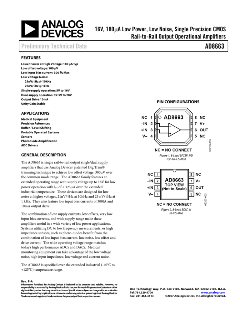
PIN CONFIGURATIONS
APPLICATIONS
Medical Equipment
Precision References
Buffer / Level Shifting
Portable Operated Systems
Sensors
Photodiode Amplification
ADC Drivers
GENERAL DESCRIPTION
Figure 1. 8-Lead LFCSP_VD
(CP-16-4 Suffix)
The AD8663 is single rail-to-rail output single/dual supply
amplifiers that use Analog Devices’ patented DigiTrim®
trimming technique to achieve low offset voltage, 300μV over
the common mode range. The AD8663 family features an
extended operating range with supply voltage up to 16V for low
power operation with ISY of < 325μA over the extended
industrial temperature. These devices are designed for low
noise at higher voltages, 21nV/√Hz at 10kHz and 23 nV/√Hz at
1 kHz. They also feature low input bias currents of 300fA and
10mA output drive.
The combination of low supply currents, low offsets, very low
input bias currents, and wide supply range make these
amplifiers useful in a wide variety of low power applications.
Systems utilizing DC to low frequency measurements, or high
impedance sensors, such as photo-diodes benefit from the
combination of low input bias current, low noise, low offset and
drive current. The wide operating voltage range matches
today’s high performance ADCs and DACs. Medical
monitoring equipment can take advantage of the low voltage
noise, high input impedance, low voltage and current noise.
Figure 2. 8-Lead SOIC_N
(R-8 Suffix)
The AD8663 is specified over the extended industrial (-40ºC to
+125ºC) temperature range.
Rev. PrA
Information furnished by Analog Devices is believed to be accurate and reliable. However, no
responsibility is assumed by Analog Devices for its use, nor for any infringements of patents or other
rights of third parties that may result from its use. Specifications subject to change without notice. No
license is granted by implication or otherwise under any patent or patent rights of Analog Devices.
Trademarks and registered trademarks are the property of their respective owners.
One Technology Way, P.O. Box 9106, Norwood, MA 02062-9106, U.S.A.
Tel: 781.329.4700
www.analog.com
Fax: 781.461.3113
©2007 Analog Devices, Inc. All rights reserved.
AD8663
Preliminary Technical Data
TABLE OF CONTENTS
Features .............................................................................................. 1
Specifications .....................................................................................3
Applications....................................................................................... 1
Absolute Maximum Ratings ............................................................5
General Description ......................................................................... 1
Thermal Resistance .......................................................................5
Pin Configurations ........................................................................... 1
ESD Caution...................................................................................5
Revision History ............................................................................... 2
Ordering Guide .............................................................................5
Specifications................................ Error! Bookmark not defined.
REVISION HISTORY
4/07—Revision 0: Initial Version
Rev. PrA | Page 2 of 5
Preliminary Technical Data
AD8663
Rev. PrA | Page 3 of 5
AD8663
Preliminary Technical Data
Rev. PrA | Page 4 of 5
Preliminary Technical Data
AD8663
ABSOLUTE MAXIMUM RATINGS
Table 1.
Parameter
Supply Voltage
Input Voltage
Differential Input Voltage
Output Short-Circuit Duration to GND
Storage Temperature Range
Operating Temperature Range
Junction Temperature Range
Lead Temperature (Soldering 60 sec)
Rating
18V
VS supply
18V
Indefinite
−65°C to +150°C
−40°C to +125°C
−65°C to +150°C
300°C
Stresses above those listed under Absolute Maximum Ratings
may cause permanent damage to the device. This is a stress
rating only; functional operation of the device at these or any
other conditions above those indicated in the operational
section of this specification is not implied. Exposure to absolute
maximum rating conditions for extended periods may affect
device reliability.
THERMAL RESISTANCE
θJA is specified for the worst-case conditions, that is, a device
soldered in circuit board for surface-mount packages.
Table 2.
Package Type
8-Lead SOIC_N
8-Lead LFCSP_VD
θJA
121
75
θJC
43
18
Unit
°C/W
°C/W
ESD CAUTION
ESD (electrostatic discharge) sensitive device. Electrostatic charges as high as 4000 V readily accumulate on
the human body and test equipment and can discharge without detection. Although this product features
proprietary ESD protection circuitry, permanent damage may occur on devices subjected to high energy
electrostatic discharges. Therefore, proper ESD precautions are recommended to avoid performance
degradation or loss of functionality.
ORDERING GUIDE
Model
AD8663ACPZ-R21
AD8663ACPZ-R71
AD8663ACPZ-RL1
AD8663ARZ1
AD8663ARZ-R71
AD8663ARZ-RL1
1
Temperature Range
−40°C to +125°C
−40°C to +125°C
−40°C to +125°C
−40°C to +125°C
−40°C to +125°C
−40°C to +125°C
Package Description
8-Lead Lead Frame Chip Scale Package [LFCSP_VD]
8-Lead Lead Frame Chip Scale Package [LFCSP_VD]
8-Lead Lead Frame Chip Scale Package [LFCSP_VD]
8-Lead Standard Small Outline Package [SOIC_N]
8-Lead Standard Small Outline Package [SOIC_N]
8-Lead Standard Small Outline Package [SOIC_N]
Z = Pb-free part.
©2007 Analog Devices, Inc. All rights reserved. Trademarks and
registered trademarks are the property of their respective owners.
PR06742-0-6/07(PrA)
Rev. PrA | Page 5 of 5
Package Option
CP-8-2
CP-8-2
CP-8-2
R-8
R-8
R-8
