Preliminary Technical Data
FEATURES
210˚C Precision Micropower
Voltage Reference
ADR225
PIN CONFIGURATION
Extreme high temperature operation
−40°C to +210°C, Ceramic flat pack (CFP)
−40°C to +175°C, SOIC package
Temperature coefficient:
20 ppm/°C, Ceramic Flat Pack (CFP)
10 ppm/°C, SOIC Package
High output current: 10 mA
Low supply current: 50 μA Max
Initial accuracy: ±2mV
Low dropout voltage
APPLICATIONS
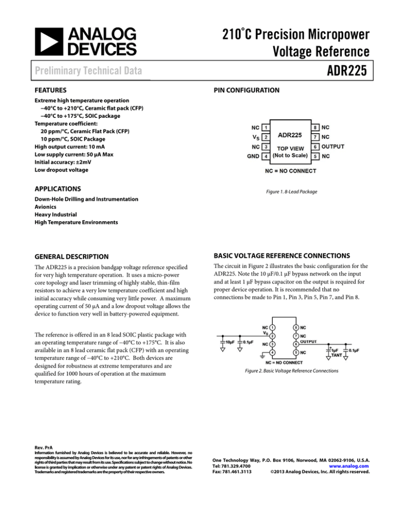
Figure 1. 8-Lead Package
Down-Hole Drilling and Instrumentation
Avionics
Heavy Industrial
High Temperature Environments
GENERAL DESCRIPTION
BASIC VOLTAGE REFERENCE CONNECTIONS
The ADR225 is a precision bandgap voltage reference specified
for very high temperature operation. It uses a micro-power
core topology and laser trimming of highly stable, thin-film
resistors to achieve a very low temperature coefficient and high
initial accuracy while consuming very little power. A maximum
operating current of 50 μA and a low dropout voltage allows the
device to function very well in battery-powered equipment.
The circuit in Figure 2 illustrates the basic configuration for the
ADR225. Note the 10 μF/0.1 μF bypass network on the input
and at least 1 μF bypass capacitor on the output is required for
proper device operation. It is recommended that no
connections be made to Pin 1, Pin 3, Pin 5, Pin 7, and Pin 8.
The reference is offered in an 8 lead SOIC plastic package with
an operating temperature range of −40°C to +175°C. It is also
available in an 8 lead ceramic flat pack (CFP) with an operating
temperature range of −40°C to +210°C. Both devices are
designed for robustness at extreme temperatures and are
qualified for 1000 hours of operation at the maximum
temperature rating.
Figure 2. Basic Voltage Reference Connections
Rev. PrA
Information furnished by Analog Devices is believed to be accurate and reliable. However, no
responsibility is assumed by Analog Devices for its use, nor for any infringements of patents or other
rights of third parties that may result from its use. Specifications subject to change without notice. No
license is granted by implication or otherwise under any patent or patent rights of Analog Devices.
Trademarks and registered trademarks are the property of their respective owners.
One Technology Way, P.O. Box 9106, Norwood, MA 02062-9106, U.S.A.
Tel: 781.329.4700
www.analog.com
Fax: 781.461.3113
©2013 Analog Devices, Inc. All rights reserved.
ADR225
Preliminary Technical Data
ELECTRICAL CHARACTERISTICS
@ VS = 3.3V, TMin< TA < TMax , unless otherwise noted.
Table 1.
Parameter
Symbol
Conditions
SUPPLY CURRENT
Isy
No load
INITIAL ACCURACY1
VO
IOUT = 0 mA
±2
±10
±2
mV
TEMPERATURE
COEFFICIENT2
TCVO/°C
IOUT = 0 mA
10
30
20
ppm/°C
LINE REGULATION
ΔVO/ΔVIN
3.0 V ≤ VS ≤ 15 V, IOUT = 0
mA
5
40
5
ppm/V
LOAD REGULATION3
ΔVO/ΔVLOAD
VS = 5.0 V, 0 mA ≤ IOUT ≤ 10
mA
10
40
10
ppm/mA
DROPOUT VOLTAGE
V S − VO
ILOAD = 10 mA
1.00
1.00
V
NOISE VOLTAGE
eN
0.1 Hz to 10 Hz
25
μV p-p
1
2
Min
Typ
Max
SOIC −40°C ≤ TA ≤ +175°C
30
50
25
For proper operation, a 1 μF capacitor is required between the output pin and the GND pin of the device.
TCVO is defined as the ratio of output change with temperature variation to the specified temperature range expressed in ppm/°C.
TCVO = (VMAX − VMIN)/VO(TMAX − TMIN)
3
Min
Typ
Max
CFP −40°C ≤ TA ≤ +210°C
35
Load regulation specification includes the effect of self-heating.
Rev. PrA | Page 2 of 3
Unit
μA
Preliminary Technical Data
ADR225
ABSOLUTE MAXIMUM RATINGS
THERMAL RESISTANCE
Table 2.
Parameter
Supply Voltage
Output to GND
Storage Temperature Range
Operating Temperature Range
SOIC Package
CFP Package
Junction Temperature Range
SOIC Package
CFP Package
Lead Temperature (Soldering 60 sec)
Rating
−0.3 V to +15 V
−0.3 V to VS + 0.3 V
−65°C to +150°C
−40°C to +175°C
−40°C to +210°C
−40°C to +175°C
−40°C to +210°C
300°C
Stresses above those listed under Absolute Maximum Ratings
may cause permanent damage to the device. This is a stress
rating only; functional operation of the device at these or any
other conditions above those indicated in the operational
section of this specification is not implied. Exposure to absolute
maximum rating conditions for extended periods may affect
device reliability.
©2013 Analog Devices, Inc. All rights reserved. Trademarks and
registered trademarks are the property of their respective owners.
PR11525-0-7/13(PrA)
θJA is specified for worst-case conditions; that is, θJA is specified
s specified for the device soldered in the circuit board.
Table 3.
Package Type
8-Lead SOIC (R)
8-Lead CFP (RU)
ESD CAUTION
θJA
158
TBD
θJC
43
TBD
Unit
°C/W
°C/W
