CMT01N60
advertisement

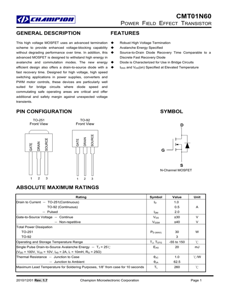
CMT01N60 POWER FIELD EFFECT TRANSISTOR GENERAL DESCRIPTION FEATURES This high voltage MOSFET uses an advanced termination Robust High Voltage Termination scheme to provide enhanced voltage-blocking capability Avalanche Energy Specified without degrading performance over time. In addition, this Source-to-Drain Diode Recovery Time Comparable to a advanced MOSFET is designed to withstand high energy in Discrete Fast Recovery Diode avalanche and commutation modes. The new energy Diode is Characterized for Use in Bridge Circuits efficient design also offers a drain-to-source diode with a IDSS and VDS(on) Specified at Elevated Temperature fast recovery time. Designed for high voltage, high speed switching applications in power supplies, converters and PWM motor controls, these devices are particularly well suited for bridge circuits where diode speed and commutating safe operating areas are critical and offer additional and safety margin against unexpected voltage transients. PIN CONFIGURATION SYMBOL D SOURCE DRAIN GATE SOURCE DRAIN TO-92 Front View GATE TO-251 Front View G S N-Channel MOSFET 1 2 3 2 1 3 ABSOLUTE MAXIMUM RATINGS Rating Drain to Current - TO-251(Continuous) Symbol Value ID 1.0 TO-92 (Continuous) 0.5 - Pulsed Gate-to-Source Voltage - Continue - Non-repetitive Unit A IDM 2.0 VGS ±30 V VGSM ±40 V PD (MAX) 30 W Total Power Dissipation TO-251 3 TO-92 Operating and Storage Temperature Range Single Pulse Drain-to-Source Avalanche Energy - TJ = 25℃ TJ, TSTG -55 to 150 ℃ EAS 20 mJ θJC 1.0 ℃/W θJA 62.5 TL 260 (VDD = 100V, VGS = 10V, IAS = 2A, L = 10mH, RG = 25Ω) Thermal Resistance - Junction to Case - Junction to Ambient Maximum Lead Temperature for Soldering Purposes, 1/8” from case for 10 seconds 2010/12/01 Rev. 1.7 Champion Microelectronic Corporation ℃ Page 1 CMT01N60 POWER FIELD EFFECT TRANSISTOR ORDERING INFORMATION Part Number Package CMT01N60GN251 TO-251 CMT01N60XN251* TO-251 CMT01N60GN92 TO-92 CMT01N60XN92* *Note: G : Suffix for Pb Free Product X : Suffix for Halogen Free Product TO-92 ELECTRICAL CHARACTERISTICS Unless otherwise specified, TJ = 25℃. Characteristic Drain-Source Breakdown Voltage (VGS = 0 V, ID = 250 μA) Drain-Source Leakage Current (VDS = 600 V, VGS = 0 V) (VDS = 480 V, VGS = 0 V, TJ = 125℃) Gate-Source Leakage Current-Forward (Vgsf = 30 V, VDS = 0 V) Gate-Source Leakage Current-Reverse (Vgsr =- 30 V, VDS = 0 V) Gate Threshold Voltage (VDS = VGS, ID = 250 μA) Symbol V(BR)DSS Static Drain-Source On-Resistance (VGS = 10 V, ID = 0.5A) * TO-251 TO-92 Forward Transconductance (VDS ≧ 50 V, ID = 0.5A) * Input Capacitance (VDS = 25 V, VGS = 0 V, Output Capacitance f = 1.0 MHz) Reverse Transfer Capacitance Turn-On Delay Time (VDD = 300 V, ID = 1.0 A, Rise Time VGS = 10 V, Turn-Off Delay Time RG = 18Ω) * Fall Time Total Gate Charge (VDS = 400 V, ID = 1.0 A, Gate-Source Charge VGS = 10 V)* Gate-Drain Charge Internal Drain Inductance (Measured from the drain lead 0.25” from package to center of die) Internal Drain Inductance (Measured from the source lead 0.25” from package to source bond pad) SOURCE-DRAIN DIODE CHARACTERISTICS Forward On-Voltage(1) (IS = 1.0 A, VGS = 0 V, Forward Turn-On Time dIS/dt = 100A/μs) Reverse Recovery Time CMT01N60 Typ Max Units V IDSS 1 3 uA IGSSF 100 nA IGSSR 100 nA VGS(th) Min 600 2.0 V 4.0 RDS(on) 11 Ω gFS 320 mhos Ciss Coss Crss td(on) tr td(off) tf Qg Qgs Qgd LD 210 28 4.2 8 21 18 24 8.5 1.8 4 4.5 pF pF pF ns ns ns ns nC nC nC nH LS 7.5 nH VSD ton trr ** 350 1.5 V ns ns * Pulse Test: Pulse Width ≦300μs, Duty Cycle ≦2% ** Negligible, Dominated by circuit inductance 2010/12/01 Rev. 1.7 Champion Microelectronic Corporation Page 2 CMT01N60 POWER FIELD EFFECT TRANSISTOR TYPICAL ELECTRICAL CHARACTERISTICS 2010/12/01 Rev. 1.7 Champion Microelectronic Corporation Page 3 CMT01N60 POWER FIELD EFFECT TRANSISTOR 2010/12/01 Rev. 1.7 Champion Microelectronic Corporation Page 4 CMT01N60 POWER FIELD EFFECT TRANSISTOR PACKAGE DIMENSION TO-251 2010/12/01 Rev. 1.7 Champion Microelectronic Corporation Page 5 CMT01N60 POWER FIELD EFFECT TRANSISTOR TO-92 2010/12/01 Rev. 1.7 Champion Microelectronic Corporation Page 6 CMT01N60 POWER FIELD EFFECT TRANSISTOR IMPORTANT NOTICE Champion Microelectronic Corporation (CMC) reserves the right to make changes to its products or to discontinue any integrated circuit product or service without notice, and advises its customers to obtain the latest version of relevant information to verify, before placing orders, that the information being relied on is current. A few applications using integrated circuit products may involve potential risks of death, personal injury, or severe property or environmental damage. CMC integrated circuit products are not designed, intended, authorized, or warranted to be suitable for use in life-support applications, devices or systems or other critical applications. Use of CMC products in such applications is understood to be fully at the risk of the customer. In order to minimize risks associated with the customer’s applications, the customer should provide adequate design and operating safeguards. HsinChu Headquarter Sales & Marketing 5F-1, No. 11, Park Avenue II, Science-Based Industrial Park, HsinChu City, Taiwan T E L : +886-3-567 9979 F A X : +886-3-567 9909 21F., No. 96, Sec. 1, Sintai 5th Rd., Sijhih City, Taipei County 22102, 2010/12/01 Rev. 1.7 Taiwan R.O.C T E L : +886-2-2696 3558 F A X : +886-2-2696 3559 Champion Microelectronic Corporation Page 7


