CPC3714
350V N-Channel
Depletion-Mode FET
INTEGRATED CIRCUITS DIVISION
V(BR)DSX /
V(BR)DGX
RDS(on)
(max)
IDSS (min)
Package
350VP
14
240mA
SOT-89
Features
•
•
•
•
•
•
Offers Low RDS(on) at Cold Temperatures
RDS(on) 14 max. at 25ºC
High Input Impedance
High Breakdown Voltage: 350V
Low VGS(off) Voltage: -1.6 to -3.9V
Small Package Size: SOT-89
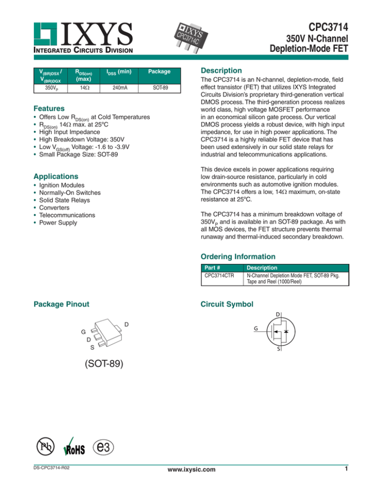
The CPC3714 is an N-channel, depletion-mode, field
effect transistor (FET) that utilizes IXYS Integrated
Circuits Division’s proprietary third-generation vertical
DMOS process. The third-generation process realizes
world class, high voltage MOSFET performance
in an economical silicon gate process. Our vertical
DMOS process yields a robust device, with high input
impedance, for use in high power applications. The
CPC3714 is a highly reliable FET device that has
been used extensively in our solid state relays for
industrial and telecommunications applications.
This device excels in power applications requiring
low drain-source resistance, particularly in cold
environments such as automotive ignition modules.
The CPC3714 offers a low, 14 maximum, on-state
resistance at 25ºC.
Applications
•
•
•
•
•
•
Description
Ignition Modules
Normally-On Switches
Solid State Relays
Converters
Telecommunications
Power Supply
The CPC3714 has a minimum breakdown voltage of
350VP and is available in an SOT-89 package. As with
all MOS devices, the FET structure prevents thermal
runaway and thermal-induced secondary breakdown.
Ordering Information
Part #
CPC3714CTR
Description
N-Channel Depletion Mode FET, SOT-89 Pkg.
Tape and Reel (1000/Reel)
Circuit Symbol
Package Pinout
D
D
G
G
D
S
S
(SOT-89)
DS-CPC3714-R02
www.ixysic.com
1
INTEGRATED CIRCUITS DIVISION
CPC3714
Absolute Maximum Ratings @ 25 ºC
Parameter
Drain-to-Source Voltage
Gate-to-Source Voltage
Pulsed Drain Current
Total Package Dissipation 1
Junction Temperature
Operational Temperature
Storage Temperature
1
Ratings
350
±15
600
1.4
150
-55 to +125
-55 to +125
Units
VP
VP
mA
W
ºC
ºC
ºC
Absolute Maximum Ratings are stress ratings. Stresses in
excess of these ratings can cause permanent damage to the
device. Functional operation of the device at conditions beyond
those indicated in the operational sections of this data sheet is
not implied.
Mounted on FR4 board 1"x1"x0.062"
Electrical Characteristics @ 25 ºC (Unless Otherwise Noted)
Parameter
Symbol
Conditions
Drain-to-Source Breakdown Voltage
V(BR)DSX
VGS= -5V, ID=100µA
350
Gate-to-Source Off Voltage
VGS(off)
IDS= 5V, ID=1mA
-1.6
Change in VGS(off) with Temperatures
Min
Typ
Max
Units
-
-
VP
-
-3.9
V
dVGS(off)/dT
VDS= 5V, ID=1mA
-
-
4.5
mV/ºC
Gate Body Leakage Current
IGSS
VGS=±15V, VDS=0V
-
-
100
nA
Drain-to-Source Leakage Current
ID(off)
Change in RDS(on) with Temperatures
-
1
A
-
1
mA
IDSS
VGS= 0V, VDS=15V
240
-
-
mA
RDS(on)
VGS= 0V, ID=240mA
-
-
14
dRDS(on)/dT
VGS= 0V, ID=240mA
-
-
1.1
%/ºC
ID= 100mA, VDS = 10V
225
-
-
m
45
100
Forward Transconductance
GFS
Input Capacitance
CISS
Common Source Output Capacitance
COSS
Reverse Transfer Capacitance
CRSS
Turn-On Delay Time
td(on)
Rise Time
VGS= -5V
VDS= 25V
f= 1MHz
td(off)
Fall time
-
tf
10
60
2
40
pF
20
VDD= 25V
ID= 150mA
VGS= 0V to -10V
Rgen= 50
tr
Turn-Off Delay Time
-
Saturated Drain-to-Source Current
Static Drain-to-Source ON-State Resistance
VGS= -5V, VDS=350V
VGS= -5V, VDS=280V, TA=125ºC
-
10
-
20
ns
50
Source-Drain Diode Voltage Drop
VSD
VGS= -5V, ISD= 150mA
-
0.6
1.8
V
Thermal Resistance (Junction to Ambient)
RJA
-
-
90
-
ºC/W
VDD
Switching Waveform & Test Circuit
RL
0V
90%
PULSE
GENERATOR
INPUT
-10V
10%
t on
t d(on)
VDS
OUTPUT
Rgen
t off
tf
t d(off)
tr
D.U.T.
90%
90%
INPUT
OUTPUT
0V
2
10%
10%
www.ixysic.com
R02
INTEGRATED CIRCUITS DIVISION
CPC3714
PERFORMANCE DATA*
250
225
200
175
150
125
100
75
50
25
0
Transfer Characteristics
(VDS=5V)
-2.0
240
-2.5
+25ºC
200
-3.0
VGS(off) (V)
VGS=-1.5V
160
+125ºC
120
80
VGS=-2.0V
1
2
3
VDS (V)
4
5
-4.0
-4.5
-5.0
0
-3.0
6
-2.5
RON vs. Temperature
(VGS=0V, ID=100mA)
-2.0
VGS (V)
-1.5
-5.5
-1.0
1.4
15
1.2
9
50
100
Temperature (ºC)
150
-55ºC
250
+25ºC
1.0
200
+125ºC
:
12
-0
300
GFS (m )
1.6
18
Power (W)
21
-50
Transconductance vs. Drain Current
(VDS=10V)
Power Dissipation
vs. Ambient Temperature
6
0.8
0.6
150
100
0.4
3
50
0.2
0
-50
-0
50
100
0
0.0
150
0
20
Temperature (ºC)
40
60
80
100 120
Ambient Temperature (ºC)
0
140
Capacitance vs. Drain Source Voltage
(VGS=-5V)
Max Rated Safe Operating Area
1
160
0.01
120
100
80
CISS
60
40
COSS
20
0.001
0.1
0
1
10
100
Drain-Source Voltage (V)
1000
RON (ȍ)
Capacitance (pF)
0.1
CRSS
0
10
20
VDS (V)
30
40
10
20
30
40 50 60
ID (mA)
70
80
90 100
On-Resistance vs. Drain Current
(VGS=0V)
140
Drain Current (A)
-3.5
-40ºC
40
0
RON (:)
VGS(off) vs. Temperature
(VDS=10V, ID=1mA)
280
VGS=-1.0V
VGS=0V
ID (mA)
ID (mA)
Output Characteristics
(TA=25ºC)
20
18
16
14
12
10
8
6
4
2
0
0
0.06
0.12
0.18
ID (A)
0.24
0.30
*The Performance data shown in the graphs above is typical of device performance. For guaranteed parameters not indicated in the written specifications, please
contact our application department.
R02
www.ixysic.com
3
INTEGRATED CIRCUITS DIVISION
CPC3714
Manufacturing Information
Moisture Sensitivity
All plastic encapsulated semiconductor packages are susceptible to moisture ingression. IXYS Integrated
Circuits Division classified all of its plastic encapsulated devices for moisture sensitivity according to
the latest version of the joint industry standard, IPC/JEDEC J-STD-020, in force at the time of product
evaluation. We test all of our products to the maximum conditions set forth in the standard, and guarantee proper
operation of our devices when handled according to the limitations and information in that standard as well as to any
limitations set forth in the information or standards referenced below.
Failure to adhere to the warnings or limitations as established by the listed specifications could result in reduced
product performance, reduction of operable life, and/or reduction of overall reliability.
This product carries a Moisture Sensitivity Level (MSL) rating as shown below, and should be handled according
to the requirements of the latest version of the joint industry standard IPC/JEDEC J-STD-033.
Device
Moisture Sensitivity Level (MSL) Rating
CPC3714C
MSL 1
ESD Sensitivity
This product is ESD Sensitive, and should be handled according to the industry standard JESD-625.
Reflow Profile
This product has a maximum body temperature and time rating as shown below. All other guidelines of J-STD-020
must be observed.
Device
Maximum Temperature x Time
CPC3714C
260ºC for 30 seconds
Board Wash
IXYS Integrated Circuits Division recommends the use of no-clean flux formulations. However, board washing to
remove flux residue is acceptable, and the use of a short drying bake may be necessary. Chlorine-based or
Fluorine-based solvents or fluxes should not be used. Cleaning methods that employ ultrasonic energy should not be
used.
4
www.ixysic.com
R02
INTEGRATED CIRCUITS DIVISION
CPC3714
MECHANICAL DIMENSIONS
CPC3714C
1.626 / 1.829
(0.064 / 0.072)
1.397 / 1.600
(0.055 / 0.063)
R 0.254
(R 0.010)
PCB Land Pattern
1.90
(0.075)
3.937 / 4.242
(0.155 / 0.167)
45º
2.286 / 2.591
(0.090 / 0.102)
2.45
(0.096)
1.40
(0.055)
Pin 1
0.889 / 1.194
(0.035 / 0.047)
0.356 / 0.483
(0.014 / 0.019)
0.432 / 0.559
(0.017 / 0.022)
50º
0.356 / 0.432
(0.014 / 0.017)
0.864 / 1.016
(0.034 / 0.040)
4.394 / 4.597
(0.173 / 0.181)
1.118 / 1.270
(0.044 / 0.050)
50º
5.00
(0.197)
1.90
(0.074)
0.432 / 0.508
(0.017 / 0.020)
0.60
(0.024)
TYP 3
2.845 / 2.997
(0.112 / 0.118)
1.422 / 1.575
(0.056 / 0.062)
2.921 / 3.073
(0.115 / 0.121)
Dimensions
mm MIN / mm MAX
(inches MIN / inches MAX)
CPC3714CTR Tape & Reel
177.8 Dia
(7.00 Dia)
5.50 ± 0.05
(0.217 ± 0.002)
Top Cover
Tape Thickness
0.102 Max
(0.004 Max)
2.00 ± 0.05
(0.079 ± 0.002)
4.00 ± 0.1
(0.157 ± 0.004)
W=12.00 ± 0.3
(0.472 ± 0.012)
B0=4.60 ± 0.1
(0.181 ± 0.004)
K0=1.80 ± 0.1
(0.071 ± 0.004)
Embossed
Carrier
1.75 ± 0.1
(0.069 ± 0.004)
A0=4.80 ± 0.1
(0.189 ± 0.004)
P=8.00 ± 0.1
(0.315 ± 0.004)
Embossment
Dimensions
mm
(inches)
For additional information please visit our website at: www.ixysic.com
IXYS Integrated Circuits Division makes no representations or warranties with respect to the accuracy or completeness of the contents of this publication and reserves the right to make
changes to specifications and product descriptions at any time without notice. Neither circuit patent licenses nor indemnity are expressed or implied. Except as set forth in IXYS Integrated
Circuits Division’s Standard Terms and Conditions of Sale, IXYS Integrated Circuits Division assumes no liability whatsoever, and disclaims any express or implied warranty, relating to
its products including, but not limited to, the implied warranty of merchantability, fitness for a particular purpose, or infringement of any intellectual property right.
The products described in this document are not designed, intended, authorized or warranted for use as components in systems intended for surgical implant into the body, or in other
applications intended to support or sustain life, or where malfunction of IXYS Integrated Circuits Division’s product may result in direct physical harm, injury, or death to a person or severe
property or environmental damage. IXYS Integrated Circuits Division reserves the right to discontinue or make changes to its products at any time without notice.
5
Specification: DS-CPC3714-R02
©Copyright 2014, IXYS Integrated Circuits Division
All rights reserved. Printed in USA.
8/1/2014


