Design of Balanced Operational Transconductance Amplifier (OTA)
advertisement

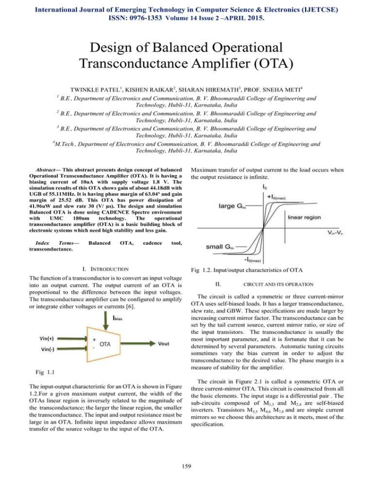
International Journal of Emerging Technology in Computer Science & Electronics (IJETCSE) ISSN: 0976-1353 Volume 14 Issue 2 –APRIL 2015. Design of Balanced Operational Transconductance Amplifier (OTA) TWINKLE PATEL1, KISHEN RAIKAR2, SHARAN HIREMATH3, PROF. SNEHA METI4 1 B.E , Department of Electronics and Communication, B. V. Bhoomaraddi College of Engineering and Technology, Hubli-31, Karnataka, India 2 B.E , Department of Electronics and Communication, B. V. Bhoomaraddi College of Engineering and Technology, Hubli-31, Karnataka, India 3 B.E , Department of Electronics and Communication, B. V. Bhoomaraddi College of Engineering and Technology, Hubli-31, Karnataka, India 4 M.Tech , Department of Electronics and Communication, B. V. Bhoomaraddi College of Engineering and Technology, Hubli-31, Karnataka, India Abstract— This abstract presents design concept of balanced Operational Transconductance Amplifier (OTA). It is having a biasing current of 10uA with supply voltage 1.8 V. The simulation results of this OTA shows gain of about 44.18dB with UGB of 55.11MHz. It is having phase margin of 63.04º and gain margin of 25.52 dB. This OTA has power dissipation of 41.96uW and slew rate 30 (V/ µs). The design and simulation Balanced OTA is done using CADENCE Spectre environment with UMC 180nm technology. The operational transconductance amplifier (OTA) is a basic building block of electronic systems which need high stability and less gain. Index Terms— transconductance. Balanced OTA, cadence Maximum transfer of output current to the load occurs when the output resistance is infinite. tool, I. INTRODUCTION Fig 1.2. Input/output characteristics of OTA The function of a transconductor is to convert an input voltage into an output current. The output current of an OTA is proportional to the difference between the input voltages. The transconductance amplifier can be configured to amplify or integrate either voltages or currents [6]. Fig 1.1 The input-output characteristic for an OTA is shown in Figure 1.2.For a given maximum output current, the width of the OTAs linear region is inversely related to the magnitude of the transconductance; the larger the linear region, the smaller the transconductance. The input and output resistance must be large in an OTA. Infinite input impedance allows maximum transfer of the source voltage to the input of the OTA. II. CIRCUIT AND ITS OPERATION The circuit is called a symmetric or three current-mirror OTA uses self-biased loads. It has a larger transconductance, slew rate, and GBW. These specifications are made larger by increasing current mirror factor. The transconductance can be set by the tail current source, current mirror ratio, or size of the input transistors. The transconductance is usually the most important parameter, and it is fortunate that it can be determined by several parameters. Automatic tuning circuits sometimes vary the bias current in order to adjust the transconductance to the desired value. The phase margin is a measure of stability for the amplifier. The circuit in Figure 2.1 is called a symmetric OTA or three current-mirror OTA. This circuit is constructed from all the basic elements. The input stage is a differential pair . The sub-circuits composed of M1,3 and M2,4 are self-biased inverters. Transistors M3,5 M4,6 M7,8 and are simple current mirrors so we choose this architecture as it meets, most of the specification. 159 International Journal of Emerging Technology in Computer Science & Electronics (IJETCSE) ISSN: 0976-1353 Volume 14 Issue 2 –APRIL 2015. MOSFET M1 M2 M3 M4 Fig 2.1. Circuit diagram of proposed OTA M5 M6 M7 M8 III. SIMULATION RESULTS Figure 2.2 Design of Balanced OTA using cadence When designing the symmetrical OTA, transistors M1 =M2, M3=M4, M5=M6,and M7=M8. This reduces the number of designable parameters to four transistor sizes and the tail current. Analysis shows that the symmetric OTA has a larger transconductance, slew rate, and GBW . The phase margin is a measure of stability for the amplifier. In most cases, the load capacitance is much larger than the capacitance at the other nodes. When this is the case, the operational transconductance amplifier has a dominant pole at the output node and two non-dominant poles at the other two nodes. Due to the symmetric behavior at the input stage, the amplifier also has a right-half plane zero. For most symmetric OTA designs, the non-dominant poles and zero are much larger than the gain-bandwidth product and degrade the phase margin by less than 10º each. This gives a typical phase margin of greater than 60º. From Fig.2.2 sizes of MOSFETs are tabulated below Fig 3.1 Amplified output on cadence tool AC analysisGain=44.18dB UGB=55.11MHz Since the AC frequency response is an important factor for any amplifier which helps to calculate the bandwidth and the gain. By operating all CMOS in to saturation region power consumption and slew rate is reduced but GBW product remains constant. 160 International Journal of Emerging Technology in Computer Science & Electronics (IJETCSE) ISSN: 0976-1353 Volume 14 Issue 2 –APRIL 2015. IV. Fig 3.2 magnitude and phase response of Balanced OTA The versatility of an OTA allows its use in many electronic systems such as filters, analog-to-digital converters, and oscillators. It finds applications mainly where in the system requires high stability. Design of OTA is of vital importance in integrated Continuous-time filters. This OTA can further be used for analog portable devices. The simulation indicates that GBW of 55.11MHz are sufficient to design modular circuit of Digital-Audio Sigma-Delta modulator. As we have shown this leads to a fast optimization program, while maintaining close matching to circuit-level simulation. I. Response for different capacitive loads: capacitance ( F) UGB (MHz) PM (deg) 100f 250f 330f 400f 500f 800f 1p 2p 129.4 70.09 55.11 47.18 39.11 25.62 20.47 10.38 36.2 55.2 62.5 65.5 68.9 76.5 78.8 84.34 II. Process corner simulation results: Process UGB in PM in deg (MHz) CONCLUSION ACKNOWLEDGMENT DC gain (dB) 44.18 44.18 44.18 44.18 44.18 44.18 44.18 44.18 tt ss 55.11 54.95 62.5 62.68 DC gain in (dB) 44.18 44.21 ff snfp 58.38 55.91 60.31 61.66 44.2 43.93 fnsp 57.38 61.11 43.87 First and foremost we would like to thank our guide Prof. Sujata Kotabagi and Prof.Sneha Meti for their moral support and frequent suggestions in developing this type of amplifier. We are very grateful to Dr.Uma Mudengudi, Head of the Department, Electronics and Communication, for her co-operation and moral support . We avail this opportunity to thank Dr.Ashok Shettar, Principal, B.V.B. College of Engineeering and Technology,Hubli, for all the facilities provided to us and supporting us in all academic endeavors. Finally, we take this opportunity to express our gratitude and respect to all those who directly or indirectly helped and encouraged us . REFERENCES [1]. L. Sungjae, B. Jagannathan, S. Narasimha, A. Chou, N. Zamdmer, J.Johnson, et al., Record RF performance of 45-nm SOI CMOS Technology,in IEEE International Electron Devices Meeting, Dec. 2007, pp. 255-258. [2]. Design of operational transconductance amplifier applying multiobjectiveoptimization , Proceedings of the argentine school of Micro-nanoelectronics,Technology and applications 2010. [3]. Adel S. Sedra, Kenneth Smith, Microelectronic Sedra/Smith, Oxford University Press. Stablility analysis: stb analysisphase margin=63.04 deg gain margin=25.52dB Circuit [4]. A Novel Design Technique of Frequenz 61 (2007) 7-8 One Stage CMOS OTA forHigh Frequency Applications By Hassan Jassim Motlak and S.Nasaem Ahmad. [5]. Razavi-Design of Analog CMOS Integrated Circuits. [6]. CMOS Analog Circuit Design-Allen ,Holberg. [7]. Design and Analysis of Two-Stage Operational Transconductance Amplifier (OTA) using Cadence tool by O. M. Saravanakumar , N. Kaleeswari , K. Rajendran . 161


