IS31LT3380 MR16 Lighting Evaluation Board Guide
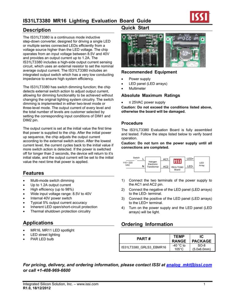
Quick Start
Description
The IS31LT3380 is a continuous mode inductive
step-down converter, designed for driving a single LED
or multiple series connected LEDs efficiently from a
voltage source higher than the LED voltage. The chip
operates from an input voltage between 8.5V and 40V
and provides an output current up to 1.2A. The
IS31LT3380 includes a high-side output current sensing
circuit, which uses an external resistor to set the nominal
average output current. The IS31LT3380 includes an
integrated output switch which has a very low conducting
impedance to ensure high system efficiency.
The IS31LT3380 has switch dimming function; the chip
detects external switch action to adjust output current,
allowing for dimming functionality to be achieved without
changing the original lighting system circuitry. The switch
dimming is implemented in either two-level mode or
three-level mode. The output current of every level and
the total number of levels are customer selected by
setting the corresponding input conditions of DIM1 and
DIM2 pin.
The output current is set at the initial value the first time
that power is supplied to the chip. After the initial power
up sequence, the chip adjusts the output current
according to the external switch action. After the lowest
current level, the current cycles back to the initial value if
more switch action is detected. If the power is switched
off for longer than 2 seconds, the device will return to it’s
initial state, and the output current will be set to the initial
value the next time that power is applied.
Recommended Equipment
Power supply
LED panel (LED arrays)
Multimeter
Absolute Maximum Ratings
≤ 25VAC power supply
Caution: Do not exceed the conditions listed above,
otherwise the board will be damaged.
Procedure
The IS31LT3380 Evaluation Board is fully assembled
and tested. Follow the steps listed below to verify board
operation.
Caution: Do not turn on the power supply until all
connections are completed.
Features
Multi-mode switch dimming
Up to 1.2A output current
High efficiency (up to 98%)
Wide input voltage range: 8.5V to 40V
Internal 40V power switch
Typical 5% output current accuracy
Inherent LED open/short-circuit protection
Thermal shutdown protection circuitry
Applications
MR16, MR11 LED spotlight
LED street lighting
PAR LED bulb
1)
2)
3)
4)
Connect the two terminals of the power supply to
the AC1 and AC2 pin.
Connect the negative of the LED panel (LED arrays)
to the LED- terminal.
Connect the positive of the LED panel (LED arrays)
to the LED+ terminal.
Turn on the power supply and the LED panel (LED
arrays) will be light.
Ordering Information
PART #
TEMP
RANGE
IC
PACKAGE
IS31LT3380_GRLS3_EBMR16
-40 °C to
105°C
SO-8
(5.0x6.0mm)
For pricing, delivery, and ordering information, please contact ISSI at analog_mkt@issi.com
or call +1-408-969-6600
Integrated Silicon Solution, Inc. – www.issi.com
R1.0, 18/12/2012
1
IS31LT3380 MR16 Lighting Evaluation Board Guide
close to the LX pin as possible with low resistance
connections to LX.
Detailed Description
LED Current Control
The nominal average output current in the LED(s) is
determined by the value of the external current sense
resistor (RS) connected between VIN and ISENSE and in is
given by: IOUT nom = 0.1/RS
The table below gives values of nominal average
output current for several preferred values of current
setting resistor (RS) in the application circuit:
RS (Ω)
0.083
0.15
0.3
Nominal average output
current (mA)
1200
667
333
RS need to be chosen as a 1% accuracy resistor with
enough power tolerance and good temperature
characteristic to ensure stable output current.
Inductor selection
Recommended inductor values are in the range 47μH
to 220μH. Higher values of inductance are
recommended at higher supply voltages and low output
current in order to minimize errors due to switching
delays, which result in increased ripple and lower
efficiency. Higher values of inductance also result in a
smaller change in output current over the supply
voltage range. The inductor should be mounted as
PCB layout consideration
VIN/GND pin
The GND of the power supply usually has some
distance between it and the chip GND pin, causing
parasitic resistance and inductance, resulting in ground
voltage bounce when the MOSFET switches. To
minimize ground bounce, the ground pin of the chip
should be soldered directly to the ground plane.
Connecting a 0.1uF capacitor between the VIN and
GND pins as close to the chip as possible minimizes
the effects of ground bounce.
LX pin
The LX pin of the chip is a fast switching node, so PCB
traces should be kept as short as possible.
Coil and decoupling capacitors
It is particularly important to mount the coil and the
input decoupling capacitor close to the chip to minimize
parasitic resistance and inductance, which will degrade
efficiency. It is also important to take account of any
trace resistance in series with current sense resistor RS
(shown as R1 on schematic diagram).
DIM pin
The DIM pin is a high impedance input, when left
floating this pin is pulled up to 3.3V by internal circuitry.
Avoid running any high voltage traces close to the DIM
pins.
Setting Dimming Current-Level
Pin Name / Setting
DESCRIPTION
DIM 1 (pin 6)
DIM 2 (pin 5)
Functionality
Dimming Levels
Floating
Floating
No Dimming
100%
Floating
GND
3 (Three) - levels of dimming
100% -- 50% -- 20%
GND
Floating
3 (Three) - levels of dimming
100% -- 60% -- 30%
GND
GND
2 (Two) - levels of dimming
100% -- 30%
The operation of the power switch and the configuration
of the DIM1 and DIM2 pins control the dimming process
as follows:
1. When DIM1 and DIM2 pins are both floating, there
is no switch dimming, and the output current is
100% of the programmed value when the power is
on.
2. When DIM1 is floating and DIM2 is GND, the
output current is:
a) 100% at power on.
b) The first switch dimming action causes the
current to change to 50%.
Integrated Silicon Solution, Inc. – www.issi.com
R1.0, 18/12/2012
3.
4.
c) A second switch dimming action causes the
current to return to 20%.
d) A fourth switch dimming action has the same
effect as the first switch dimming action.
e) Subsequent switch dimming actions causes
the cycle to continue.
When DIM1 is GND and DIM2 is floating, the
dimming sequence is as described in (2) above,
except
that
the
current
sequence
is
100%-60%-30%.
When both DIM1 and DIM2 are connected to GND,
the dimming sequence is as described in (2) above,
2
IS31LT3380 MR16 Lighting Evaluation Board Guide
except that the current sequence is 100%-30%.
If the switch is operated normally, that is, switched ON
once after being in the OFF position for a long time, or if
both the DIM1 and DIM2 pins are floating, then the
output current always starts up at the initial value of
100%.
R1
D5
D1
D1
Switch
D2
Halogen
Electronic
Transformer
AC110~220
1
ISENSE
VIN
C1
D3
C2
LX
IS31LT3380
DIM1
D4
C3
2
DIM2
GND
7
L1
8
6
5
R3
R2
Figure 1 IS31LT3380 Evaluation Board Schematic
Note: ISSI Evaluation Board does not include an Electronic Transformer or LED array
Bill of Materials
No.
1
2
3
4
5
6
7
8
Name
SMD Diode
AL Capacitor
SMD Capacitor
SMD Capacitor
SMD Resistor
SMD Resistor
SMD Resistor
SMD Inductor
Description
2A,40V
330uF,25V
0.1uF,50V
1uF,250V
0.15Ω,(1206),1%
0Ω,(0805)
0Ω,(0805)
47µH,Isat>1000mA
Ref Des.
L1
Qty.
5
1
1
2
1
1
1
1
9
IC
IS31LT3380
U1
1
Integrated Silicon Solution, Inc. – www.issi.com
R1.0, 18/12/2012
D1-D5
C1
C2
C3
R1 (RS)
R2
R3
Mfr P/N
3
IS31LT3380 MR16 Lighting Evaluation Board Guide
PCB Layout
Figure 2 PCB Layout- Top Layer
Figure 3
PCB Layout-Bottom Layer
Copyright © 2011 Integrated Silicon Solution, Inc. All rights reserved. ISSI reserves the right to make changes to this
specification and its products at any time without notice. ISSI assumes no liability arising out of the application or
use of any information, products or services described herein. Customers are advised to obtain the latest version of
this device specification before relying on any published information and before placing orders for products.
Integrated Silicon Solution, Inc. does not recommend the use of any of its products in life support applications where
the failure or malfunction of the product can reasonably be expected to cause failure of the life support system or to
significantly affect its safety or effectiveness. Products are not authorized for use in such applications unless
Integrated Silicon Solution, Inc. receives written assurance to its satisfaction, that:
a.) the risk of injury or damage has been minimized;
b.) the user assume all such risks; and
c.) potential liability of Integrated Silicon Solution, Inc is adequately protected under the circumstances
Integrated Silicon Solution, Inc. – www.issi.com
R1.0, 18/12/2012
4
