SG1548
QUAD POWER FAULT MONITOR
Description
Features
The SG1548 is an integrated circuit capable of monitoring
up to four positive DC supply voltages simultaneously for
overvoltage and undervoltage fault conditions. An on-chip
inverting op amp also allows monitoring one negative DC
voltage. The fault tolerance window is accurately
programmable from ±5% to ±40% using a simple divider
network on the 2.5V reference. A single external capacitor
sets the fault indication delay, eliminating false outputs
due to switching noise, logic transition current spikes, and
short-term AC line interruptions.
An additional comparator referenced to 2.5V allows the
AC line to be monitored for undervoltage conditions or for
generation of a line clock. The comparator can also be
used for programmable undervoltage lockout in a
switching power supply. Uncommitted collector and
emitter outputs permit both inverting and non-inverting
operation. External availability of the precision 2.5V
reference and open-collector logic outputs permit
expansion to monitor additional voltage using available
open-collector quad comparators.
Monitors Four DC Voltages and the AC Line
Precision 2.5V ±1% Low-drift Reference
Fault Tolerance Adjustable from ±5% to ±40%
±3% Trip Threshold Tolerance over Temperature
Separate 10mA, 40V Overvoltage, Undervoltage,
and AC line Fault Outputs
Fault Delay Programmable with a Single Capacitor
30mV Comparator Hysteresis to Prevent Oscillations
On-Chip Inverting Op-Amp for Negative Voltage
Open-Collector Output Logic or Expandability
Operation from 4.5V to 40V Supply
High Reliability Features
Following are the high reliability features of SG1548:
Available to MIL-STD-883, ¶ 1.2.1
Radiation data available
MSC-AMS level "S" processing available
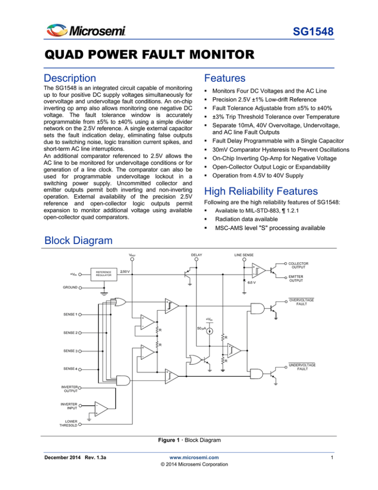
Block Diagram
Figure 1 · Block Diagram
December 2014 Rev. 1.3a
www.microsemi.com
© 2014 Microsemi Corporation
1
QUAD POWER FAULT MONITOR
Connection Diagrams and Ordering Information
Ambient
Temperature
Type
-55°C to 125°C
J
Package
16-PIN
CERAMIC
DIP
-25°C to 85°C
Part Number
Packaging
Type
SG1548J-883B
CERDIP
N
0°C to 70°C
-25°C to 85°C
DW
0°C to 70°C
16-PIN
SMALLOUTLINE
WIDE
BODY
LOWER THRESHOLD
GROUND
1
16
2
15
V REF
+V IN
3
14
4
13
LINE SENSE
5
12
EMITTER OUTPUT
COLLECTOR OUTPUT
6
11
INV. OUTPUT
INV. INPUT
SENSE 4
SENSE 3
SENSE 2
SENSE 1
7
10
U.V. FAULT
DELAY
8
9
O.V. FAULT
SG1548J
SG2548N*
16-PIN
PLASTIC
DIP
Connection Diagram
PDIP
N package: Pb-free / RoHS 100% Matte Tin Lead Finish
SG3548N*
1
16
2
15
V REF
+V IN
LINE SENSE
EMITTER OUTPUT
COLLECTOR OUTPUT
3
14
INV. OUTPUT
INV. INPUT
SENSE 4
4
13
SENSE 3
5
12
6
11
7
10
SENSE 2
SENSE 1
U.V. FAULT
DELAY
8
9
O.V. FAULT
LOWER THRESHOLD
GROUND
SG2548DW*
SOWB
SG3548DW*
DW package: Pb-free / RoHS 100% Matte Tin Lead Finish
-55°C to 125°C
L
20-PIN
CERAMIC
(LCC)
SG1548L-883B
CLCC
SG1548L
1. N.C.
2. LOWER THRESHOLD
3. GROUND
4
4. V REF
5
5. +V IN
6. N.C.
6
7. LINE SENSE
7
8. EMITTER OUTPUT
8
9. COLLECTOR
OUTPUT
10.DELAY
3
2
1
20 19
18
17
16
15
14
9
10 11 12 13
11.
12.
13.
14.
15.
16.
17.
18.
19.
20.
N.C.
O.V. FAULT
U.V. FAULT
SENSE 1
SENSE 2
N.C.
SENSE 3
SENSE 4
INV. INPUT
INV. OUTPUT
Notes:
1. Contact factory for DESC product availability.
2. All parts are viewed from the top.
3. Hermetic Packages J & L use Pb37/Sn63 hot solder lead finish, contact factory for availability of RoHS versions.
*RoHS Compliant
2
Absolute Maximum Ratings1
Absolute Maximum Ratings1
Value
Units
40
V
40
-0.3V to 6.0V
V
V
Fault Output Sink Current
Line Sense Input Current
20
±1
mA
mA
Inverting Op Amp Input Current
Inverting Op Amp Output Current
-5
25
mA
mA
Operating Junction Temperature
Hermetic (J, L Packages)
150
°C
150
-65 to 150
°C
°C
Parameter
Supply Voltage (+VIN)
Fault Output Collector Voltage
Sense Input Voltage Range
Plastic (N, DW Packages)
Storage Temperature Range
Lead Temperature
300
Notes:
1. Values beyond which damage may occur.
2. Pb-free / RoHS Peak Package Solder Reflow Temp. (40 second max. exposure). 260°C (+0, -5)
°C
Thermal Data
Value
Units
Thermal Resistance-Junction to Case, θJC
Thermal Resistance-Junction to Ambient, θJA
30
80
°C/W
°C/W
N Package
Thermal Resistance-Junction to Case, θJC
Parameter
J Package
40
°C/W
Thermal Resistance-Junction to Ambient, θJA
DW Package
65
°C/W
Thermal Resistance-Junction to Case, θJC
Thermal Resistance-Junction to Ambient, θJA
40
95
°C/W
°C/W
L Package
Thermal Resistance-Junction to Case, θJC
35
°C/W
Thermal Resistance-Junction to Ambient, θJA
120
°C/W
Notes:
1. Junction Temperature Calculation: TJ = TA + (PD × θJA).
2. The above numbers for θJC are maximums for the limiting thermal resistance of the package in a standard mounting
configuration. The θJA numbers are meant to be guidelines for the thermal performance of the device/pc-board system. All of
the above assume no ambient airflow.
3
QUAD POWER FAULT MONITOR
Recommended Operating Conditions1
Supply Voltage Range
±25% Maximum Fault Window
±40% Maximum Fault Window
Lower Threshold Input Range
(2)
Fault Tolerance Window Range
Fault Output Sink Current Range
Line Sense Output Current Range
Voltage Reference Output Current
Operating Ambient Temperature Range
SG1548
SG2548
SG3548
Notes:
1. Range over which the device is functional.
2. Limited by inverter amplifier positive swing at -55°C.
4
Value
Units
4.5 to 35
V
5.0 to 35
1.5 to 2.45
V
V
±5 to ±40
0 to 10
%
mA
0 to 10
0 to 10
mA
mA
-55 to 125
°C
-25 to 85
0 to 70
°C
°C
Electrical Characteristics
Electrical Characteristics
Unless otherwise specified, these specifications apply over the operating ambient temperatures for SG1548
with -55°C ≤ TA ≤ 125°C, SG2548 with -25°C ≤ TA ≤ 85°C, SG3548 with 0°C ≤ TA ≤ 70°C, and +VIN = 15V.
Low duty cycle pulse testing techniques are used which maintains junction and case temperatures equal to
the ambient temperature.
Parameter
Supply Section
Supply Current
(1)
Reference Section
Output Voltage
Test Conditions
SG1548/2548
Min Typ Max
SG3548
Min
Typ
Max
Units
4.8
4.8
10
mA
2.500
1
3
25
2.525
2.550
5
10
50
V
V
mV
mV
mA
-0.4
-2.0
µA
2.625
3.500
2.375
1.500
±0.6
100
2.704
3.606
2.447
1.545
±2.0
V
V
V
V
µA
dB
+VIN = 40V
TJ= 25°C
Over Temperature
+VIN = 4.5V to 35V
IL = 0 to 10mA
VREF = 0V
Line Regulation
Load Regulation
Short Circuit Current
Fault Window Generator Section
Input Bias Current
V PIN 1 = 1.5V to 2.45V
DC Sense Inputs Section
Overvoltage Threshold
VPIN 1 = 0.95 x VREF
V PIN 1 = 0.60 x VREF
Undervoltage Threshold
V PIN 1 = 0.95 x VREF
V PIN 1 = 0.60 x VREF
Input Bias Current
V SENSE = 1.5V to 3.5V
Threshold Supply Rejection
+V IN = 4.5V to 35V
Fault Delay Section
Comparator Threshold
Comparator Hysteresis
Delay Charging Current
VPIN 8 = 0V
On Saturation Voltage
I PIN 8 = 0mA
OFF Clamp Voltage
I PIN 8 = 0mA
(2)
Inverting Op Amp Section
Input Offset Voltage
Input Bias Current
Output High Voltage
ISOURCE = 5mA
Output Low Voltage
ISINK = 5mA
Large Signal Voltage Gain
RL = 10k
Output Source Current
Power Supply Rejection Ratio
+VIN = 4.5V to 35V
AC Line Sense Section
Comparator Threshold
V PIN 5 = Low to High
Comparator Hysteresis
Input Bias Current
V PIN 5 = 2.5V
Collector Leakage Current
VCE = 40V
Collector Saturation Voltage
IC= 10mA
Emitter Output Voltage
IE = 10mA
Diode Clamp Voltage
I PIN 5 = 1mA
I PIN 5 = -1mA
Fault Logic Outputs (Each output)
Collector Leakage Current
VC = 40V
Collector Saturation Voltage
IC = 10mA
Notes:
1. IL = 0mA
2. +VIN = 4.5V.
10
2.475 2.500 2.525
2.450
2.550
1
5
3
10
10
25
50
2.547
3.396
2.304
1.455
60
-0.4
-2.0
2.625
3.500
2.375
1.500
±0.6
100
2.704
3.606
2.447
1.545
±2.0
3.2
72
5
72
2.547
3.396
2.304
1.455
1.200
32.5
15
-1.0
3.2
1.9
25
2.440 2.500 2.560
25
1
2
1
10
0.2
0.5
12
13
6.0
7.5
-0.3
-1.0
1
0.2
10
60
1.200 1.250 1.300
25
32.5
50
67.5
0.1
0.2
+3.2 +3.6
2
-0.3
3.5
1.0
100
15
100
2.475
2.450
10
0.5
72
5
72
2.440
12
6.0
-0.3
1.250 1.300
25
50
67.5
0.1
0.2
+3.2 +3.6
V
mV
µA
V
V
2
-0.3
3.5
1.0
100
15
100
15
-1.0
mV
µA
V
V
dB
mA
dB
2.500
25
1
1
0.2
13
2.560
1.9
25
2
10
0.5
7.5
-1.0
1
0.2
10
0.5
V
mV
µA
µA
V
V
V
V
µA
V
5
QUAD POWER FAULT MONITOR
Application Information
Setting the Fault Tolerance Window
The fault tolerance window is set by applying a voltage less than the +2.50Vreference to the Lower
Threshold input (Pin 1). The voltage is obtained by a resistor divider from the reference (Pin 3) to ground. If
±5% tolerance is desired, then 95% of the reference (+2.375V) is applied to Pin 1. If ±40% is wanted, then
60% of the reference (+1.50V) is applied. In the example on the back page, the tolerance is ±5%. The
nominal overvoltage and undervoltage thresholds are centered about the reference at +2.625V and +2.375V
(+2.500V ±0.125V).
Scaling the Monitored Supply Voltages
Each positive voltage to be monitored is divided down to +2.50V with a resistor network and connected to
one of the Sense inputs. Unused Sense inputs should be connected to the reference. This will not increase
the bias current. A variation of the monitored voltages out of the programmed tolerance range will cause the
appropriate overvoltage or undervoltage fault output to switch LOW. The effective tolerance on any input
may be broadened with an additional resistor to the voltage reference. The example on the back page
shows a ±10% tolerance on the +5Vsupply although the SG1548 is programmed for a ±5% tolerance. The
procedure for calculating the resistor value is found in the SG1548 Application Note.
Monitoring a Negative Voltage
A negative voltage can be converted to a positive one and simultaneously scaled to +2.50V by using the
internal operational amplifier as an inverter. Only an input resistor and feedback resistor are required.
Setting the Fault Delay
A single capacitor at the Delay pin sets the time an out-of tolerance fault must persist before a fault is
actually declared. This feature allows switching noise on the supplies to be rejected. The delay time is given
by: Delay = 25ms/µF.
AC Line Monitoring
The AC line voltage can be monitored for single-cycle dropouts with the few components shown in the
example. A half-wave rectifier charges the capacitor on positive line cycles. After the positive peak and
during the negative line cycle the capacitor discharges from a fixed voltage controlled by the internal Zener
diode. If a positive cycle is missing, the capacitor discharges to below the +2.5V trip point of the comparator,
causing the output transistor to turn on.
6
Application Information
Application Example
In this example, the SG1548 simultaneously monitors four DC voltages: +5V, +24V, and ±15V. Three
different fault tolerances are programmed: ±5% on the two 15V supplies, ±10% on the +5V supply, and
±20% on the +24V supply. The 5µF delay capacitor provides 125 milliseconds of fault delay.
BIAS SUPPLY
VREF
10.7 k
374
SG1548
+24 V ± 20%
11
SENSE 1
+VIN
4
12
SENSE 2
O.V.FAULT
9
OVERVOLTAGE
13
SENSE 3
U.V.FAULT
10
UNDERVOLTAGE
15
INV. IN
VREF
3
1.24 k
1.24 k
619
+5 V ± 10%
1.24 k
6.24 k
+15 V ± 5%
1.24 k
15 k
-15 V ± 5%
124 Ω
2.49 k
16
INV. OUT
L. THRESHOLD
1
2.37 k
14
SENSE 4
DELAY
8
5 µF
3.3 k
120 VAC
60 Hz
6 VRMS
180 k
5 LINE SENSE COLLECTOR 7
LINE FAULT
0.1
2 GROUND
EMITTER 6
Figure 2 · Application Example
7
QUAD POWER FAULT MONITOR
Package Outline Dimensions
Controlling dimensions are in inches, metric equivalents are shown for general information.
A
b
b2
MILLIMETERS
MIN
MAX
5.08
0.38
0.51
1.04
1.65
INCHES
MAX
0.200
0.015
0.020
0.045
0.065
c
D
0.20
19.30
0.008
0.760
E
e
5.59
7.11
2.54 BSC
0.220
0.280
0.100 BSC
eA
H
7.37
0.63
7.87
1.78
0.290
0.025
0.310
0.070
L
α
3.18
-
5.08
15°
0.125
-
0.200
15°
Q
0.51
1.02
0.020
0.040
Dim
D
16
9
1
8
E
eA
b2
Q A
Seating Plane
L c
H
α
b
e
0.38
19.94
MIN
0.015
0.785
*
Note:
Dimensions do not include protrusions; these shall
not exceed 0.155mm (.006”) on any side. Lead
dimension shall not include solder coverage.
Figure 3 · J 16-Pin Ceramic Dip
Dim
MILLIMETERS
MIN
A
A1
D
A2
E1
1
b1
E
MIN
5.33
0.38
MAX
0.210
0.015
3.30 Typ.
0.130 Typ.
b
0.36
0.56
0.014
0.022
b1
1.14
1.78
0.045
0.070
c
0.20
0.36
0.008
0.014
D
18.67
19.69
0.735
0.775
e
A2
MAX
INCHES
2.54 BSC
0.100 BSC
A
c
A1
L
e
SEATING PLANE
b
θ
E
7.62
8.26
0.300
0.325
E1
6.10
7.11
0.240
0.280
L
2.92
0.381
0.115
0.150
θ
-
15°
-
15°
Note:
Dimensions do not include mold flash or protrusions;
these shall not exceed 0.155mm (.006”) on any side.
Lead dimension shall not include solder coverage.
Figure 11 · N 16-Pin Plastic Dip
8
Package Outline Dimensions (continued)
Package Outline Dimensions (continued)
Controlling dimensions are in inches, metric equivalents are shown for general information.
Dim
D
16
9
E
H
8
1
e
B
L
A2
A
SEATING PLANE
c
MILLIMETERS
INCHES
A
MIN
2.06
MAX
2.65
MIN
0.081
MAX
0.104
A1
A2
0.10
2.03
0.30
2.55
0.004
0.080
0.012
0.100
B
c
0.33
0.23
0.51
0.32
0.013
0.009
0.020
0.013
D
E
10.08
7.40
10.50
7.60
0.397
0.291
0.413
0.299
e
H
1.27 BSC
10.00
10.65
0.05 BSC
0.394
0.419
L
Θ
0.40
0°
1.27
8°
0.016
0°
0.050
8°
*LC
−
0.10
−
0.004
Note:
A1
1. Controlled dimensions are in mm, inches are for
reference only.
2. Dimensions do not include mold flash or protrusions;
these shall not exceed 0.155mm (.006”) on any side.
Lead dimension shall not include solder coverage.
Figure 12 · DW 16-Pin Plastic Wide-body SOIC
E3
D
Dim
E
A
A1
INCHES
MAX
MIN
MAX
D/E
8.64
9.14
0.340
0.360
E3
-
8.128
-
0.320
e
1.270 BSC
0.050 BSC
B1
0.635 TYP
0.025 TYP
L
1.02
1.52
0.040
0.060
A
1.626
2.286
0.064
0.090
h
L2
MILLIMETERS
MIN
1.016 TYP
0.040 TYP
L
A1
8
3
1.372
1.68
A2
-
L2
1.91
B3
0.054
0.066
1.168
-
0.046
2.41
0.075
0.95
0.203R
0.008R
1
Note:
13
h
A2
18
B1
e
B3
All exposed metalized area shall be gold plated
60 micro-inch minimum thickness over nickel
plated unless otherwise specified in purchase
order.
Figure 13 · 20-Pin Ceramic Leadless Chip Carrier
9
Microsemi Corporation (Nasdaq: MSCC) offers a comprehensive portfolio of semiconductor
and system solutions for communications, defense & security, aerospace and industrial
markets. Products include high-performance and radiation-hardened analog mixed-signal
integrated circuits, FPGAs, SoCs and ASICs; power management products; timing and
synchronization devices and precise time solutions, setting the world’s standard for time; voice
processing devices; RF solutions; discrete components; security technologies and scalable
anti-tamper products; Power-over-Ethernet ICs and midspans; as well as custom design
capabilities and services. Microsemi is headquartered in Aliso Viejo, Calif., and has
approximately 3,400 employees globally. Learn more at www.microsemi.com.
Microsemi Corporate Headquarters
One Enterprise, Aliso Viejo,
CA 92656 USA
Within the USA: +1 (800) 713-4113
Outside the USA: +1 (949) 380-6100
Sales: +1 (949) 380-6136
Fax: +1 (949) 215-4996
E-mail: sales.support@microsemi.com
© 2014 Microsemi Corporation. All
rights reserved. Microsemi and the
Microsemi logo are trademarks of
Microsemi Corporation. All other
trademarks and service marks are the
property of their respective owners.
Microsemi makes no warranty, representation, or guarantee regarding the information contained herein or
the suitability of its products and services for any particular purpose, nor does Microsemi assume any
liability whatsoever arising out of the application or use of any product or circuit. The products sold
hereunder and any other products sold by Microsemi have been subject to limited testing and should not
be used in conjunction with mission-critical equipment or applications. Any performance specifications are
believed to be reliable but are not verified, and Buyer must conduct and complete all performance and
other testing of the products, alone and together with, or installed in, any end-products. Buyer shall not rely
on any data and performance specifications or parameters provided by Microsemi. It is the Buyer's
responsibility to independently determine suitability of any products and to test and verify the same. The
information provided by Microsemi hereunder is provided "as is, where is" and with all faults, and the entire
risk associated with such information is entirely with the Buyer. Microsemi does not grant, explicitly or
implicitly, to any party any patent rights, licenses, or any other IP rights, whether with regard to such
information itself or anything described by such information. Information provided in this document is
proprietary to Microsemi, and Microsemi reserves the right to make any changes to the information in this
document or to any products and services at any time without notice.
SG1548.1/12.14

