Low Skew, 1:6 Crystal-to- LVCMOS/
LVTTL Fanout Buffer
ICS83905
DATA SHEET
General Description
Features
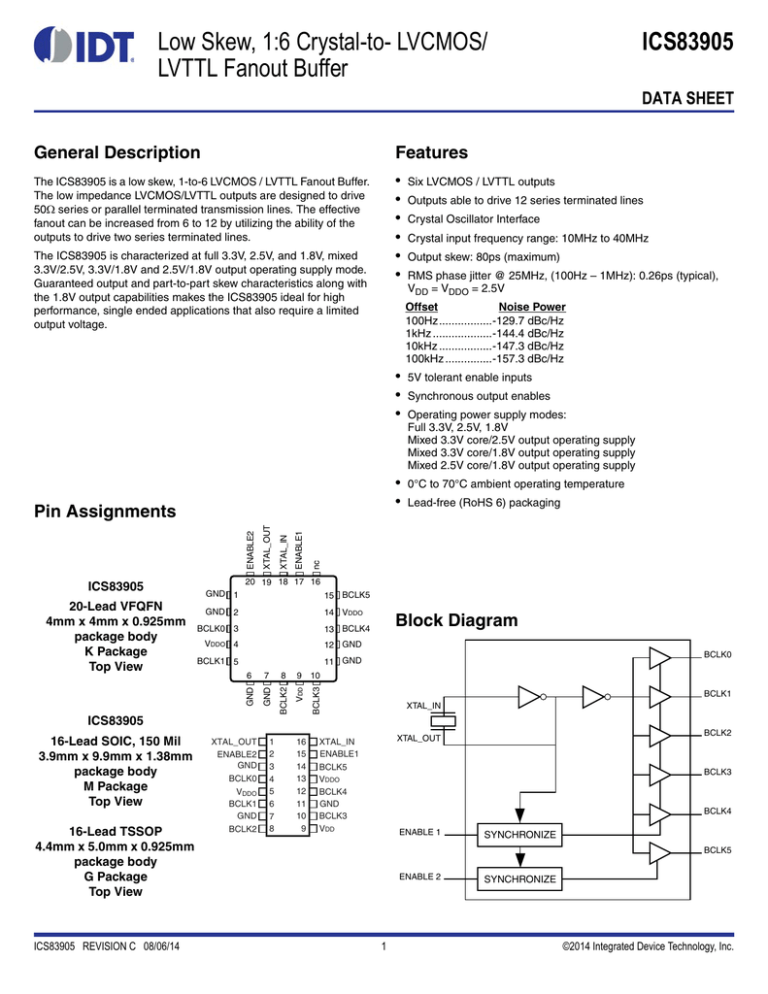
The ICS83905 is a low skew, 1-to-6 LVCMOS / LVTTL Fanout Buffer.
The low impedance LVCMOS/LVTTL outputs are designed to drive
50 series or parallel terminated transmission lines. The effective
fanout can be increased from 6 to 12 by utilizing the ability of the
outputs to drive two series terminated lines.
•
•
•
•
•
•
The ICS83905 is characterized at full 3.3V, 2.5V, and 1.8V, mixed
3.3V/2.5V, 3.3V/1.8V and 2.5V/1.8V output operating supply mode.
Guaranteed output and part-to-part skew characteristics along with
the 1.8V output capabilities makes the ICS83905 ideal for high
performance, single ended applications that also require a limited
output voltage.
ENABLE1
Crystal input frequency range: 10MHz to 40MHz
Output skew: 80ps (maximum)
RMS phase jitter @ 25MHz, (100Hz – 1MHz): 0.26ps (typical),
VDD = VDDO = 2.5V
•
•
•
5V tolerant enable inputs
•
•
0°C to 70°C ambient operating temperature
Synchronous output enables
Operating power supply modes:
Full 3.3V, 2.5V, 1.8V
Mixed 3.3V core/2.5V output operating supply
Mixed 3.3V core/1.8V output operating supply
Mixed 2.5V core/1.8V output operating supply
Lead-free (RoHS 6) packaging
nc
XTAL_IN
XTAL_OUT
ENABLE2
Crystal Oscillator Interface
20 19 18 17 16
GND 1
15 BCLK5
GND 2
14 VDDO
BCLK0 3
Block Diagram
13 BCLK4
7
8
9 10
XTAL_OUT
ENABLE2
GND
1
2
3
4
5
6
7
8
BCLK0
BCLK3
6
VDD
11 GND
BCLK2
12 GND
BCLK1 5
GND
VDDO 4
GND
20-Lead VFQFN
4mm x 4mm x 0.925mm
package body
K Package
Top View
Outputs able to drive 12 series terminated lines
Noise Power
Offset
100Hz.................-129.7 dBc/Hz
1kHz ...................-144.4 dBc/Hz
10kHz .................-147.3 dBc/Hz
100kHz ...............-157.3 dBc/Hz
Pin Assignments
ICS83905
Six LVCMOS / LVTTL outputs
BCLK1
XTAL_IN
ICS83905
16-Lead SOIC, 150 Mil
3.9mm x 9.9mm x 1.38mm
package body
M Package
Top View
16-Lead TSSOP
4.4mm x 5.0mm x 0.925mm
package body
G Package
Top View
ICS83905 REVISION C 08/06/14
BCLK0
VDDO
BCLK1
GND
BCLK2
16
15
14
13
12
11
10
9
BCLK2
XTAL_OUT
XTAL_IN
ENABLE1
BCLK5
VDDO
BCLK4
GND
BCLK3
VDD
BCLK3
BCLK4
ENABLE 1
SYNCHRONIZE
BCLK5
ENABLE 2
1
SYNCHRONIZE
©2014 Integrated Device Technology, Inc.
ICS83905 DATA SHEET
Pin Descriptions and Characteristics
Table 1. Pin Descriptions
Name
Type
XTAL_OUT
Output
Description
Crystal oscillator interface. XTAL_OUT is the output.
XTAL_IN
Input
Crystal oscillator interface. XTAL_IN is the input.
ENABLE1, ENABLE2
Input
Clock enable. LVCMOS/LVTTL interface levels. See Table 3.
BCLK0, BCLK1, BCLK2,
BCLK3, BCLK4, BCLK5
Output
Clock outputs. LVCMOS/LVTTL interface levels.
GND
Power
Power supply ground.
VDD
Power
Power supply pin.
VDDO
Power
Output supply pin.
nc
Unused
No connect.
Table 2. Pin Characteristics
Symbol
Parameter
CIN
Input Capacitance
CPD
Power Dissipation
Capacitance
(per output)
ROUT
Test Conditions
Minimum
Typical
Maximum
4
Output Impedance
Units
pF
VDDO = 3.465V
19
pF
VDDO = 2.625V
18
pF
VDDO = 2.0V
16
pF
VDDO = 3.3V ± 5%
7
VDDO = 2.5V ± 5%
7
VDDO = 1.8V ± 0.2V
10
Function Table
Table 3. Clock Enable Function Table
Control Inputs
Outputs
ENABLE 1
ENABLE2
BCLK[0:4]
BCLK5
0
0
LOW
LOW
0
1
LOW
Toggling
1
0
Toggling
LOW
1
1
Toggling
Toggling
BCLK5
BCLK0:4
ENABLE2
ENABLE1
Figure 1. Enable Timing Diagram
LOW SKEW, 1:6 CRYSTAL-TO- LVCMOS/ LVTTL FANOUT BUFFER
2
REVISION C 08/06/14
ICS83905 DATA SHEET
Absolute Maximum Ratings
NOTE: Stresses beyond those listed under Absolute Maximum Ratings may cause permanent damage to the device. These ratings are stress
specifications only. Functional operation of product at these conditions or any conditions beyond those listed in the DC Characteristics or AC
Characteristics is not implied. Exposure to absolute maximum rating conditions for extended periods may affect product reliability.
Item
Rating
Supply Voltage, VDD
4.6V
Inputs, VI
-0.5V to VDD + 0.5V
Outputs, VO
-0.5V to VDDO+ 0.5V
Package Thermal Impedance, JA
16-Lead SOIC package
16-Lead TSSOP package
20-Lead VFQFN package
78.8C/W (0 mps)
100.3C/W (0 mps)
57.5C/W (0 mps)
Storage Temperature, TSTG
-65C to 150C
DC Electrical Characteristics
Table 4A. Power Supply DC Characteristics, VDD = VDDO = 3.3V ± 5%, TA = 0°C to 70°C
Symbol
Parameter
VDD
Test Conditions
Minimum
Typical
Maximum
Units
Power Supply Voltage
3.135
3.3
3.465
V
VDDO
Output Supply Voltage
3.135
3.3
3.465
V
IDD
Power Supply Current
ENABLE [1:2] = 00
10
mA
IDDO
Output Supply Current
ENABLE [1:2] = 00
5
mA
Table 4B. Power Supply DC Characteristics, VDD = VDDO = 2.5V ± 5%, TA = 0°C to 70°C
Symbol
Parameter
VDD
Test Conditions
Minimum
Typical
Maximum
Units
Power Supply Voltage
2.375
2.5
2.625
V
VDDO
Output Supply Voltage
2.375
2.5
2.625
V
IDD
Power Supply Current
ENABLE [1:2] = 00
8
mA
IDDO
Output Supply Current
ENABLE [1:2] = 00
4
mA
Table 4C. Power Supply DC Characteristics, VDD = VDDO = 1.8V ± 0.2V, TA = 0°C to 70°C
Symbol
Parameter
VDD
Minimum
Typical
Maximum
Units
Power Supply Voltage
1.6
1.8
2.0
V
VDDO
Output Supply Voltage
1.6
1.8
2.0
V
IDD
Power Supply Current
ENABLE [1:2] = 00
5
mA
IDDO
Output Supply Current
ENABLE [1:2] = 00
3
mA
REVISION C 08/06/14
Test Conditions
3
LOW SKEW, 1:6 CRYSTAL-TO- LVCMOS/ LVTTL FANOUT BUFFER
ICS83905 DATA SHEET
Table 4D. Power Supply DC Characteristics, VDD = 3.3V ± 5%, VDDO = 2.5V ± 5%, TA = 0°C to 70°C
Symbol
Parameter
VDD
Test Conditions
Minimum
Typical
Maximum
Units
Power Supply Voltage
3.135
3.3
3.465
V
VDDO
Output Supply Voltage
2.375
2.5
2.625
V
IDD
Power Supply Current
ENABLE [1:2] = 00
10
mA
IDDO
Output Supply Current
ENABLE [1:2] = 00
4
mA
Table 4E. Power Supply DC Characteristics, 3.3V ± 5%, VDDO = 1.8V ± 0.2V, TA = 0°C to 70°C
Symbol
Parameter
VDD
Test Conditions
Minimum
Typical
Maximum
Units
Power Supply Voltage
3.135
3.3
3.465
V
VDDO
Output Supply Voltage
1.6
1.8
2.0
V
IDD
Power Supply Current
ENABLE [1:2] = 00
10
mA
IDDO
Output Supply Current
ENABLE [1:2] = 00
3
mA
Table 4F. Power Supply DC Characteristics, VDD = 2.5V ± 5%, VDDO = 1.8V ± 0.2V, TA = 0°C to 70°C
Symbol
Parameter
VDD
Test Conditions
Minimum
Typical
Maximum
Units
Power Supply Voltage
2.375
2.5
2.625
V
VDDO
Output Supply Voltage
1.6
1.8
2.0
V
IDD
Power Supply Current
ENABLE [1:2] = 00
8
mA
IDDO
Output Supply Current
ENABLE [1:2] = 00
3
mA
LOW SKEW, 1:6 CRYSTAL-TO- LVCMOS/ LVTTL FANOUT BUFFER
4
REVISION C 08/06/14
ICS83905 DATA SHEET
Table 4G. LVCMOS/LVTTL DC Characteristics, TA = 0°C to 70°C
Symbol
Parameter
VIH
Input High
Voltage
VIL
VOH
VOL
Input Low
Voltage
ENABLE1,
ENABLE2
ENABLE1,
ENABLE2
Output High Voltage
Output Low Voltage; NOTE 1
Test Conditions
Minimum
VDD = 3.3V ± 5%
Typical
Maximum
Units
2
VDD + 0.3
V
VDD = 2.5V ± 5%
1.7
VDD + 0.3
V
VDD = 1.8V ± 0.2V
0.65 * VDD
VDD + 0.3
V
VDD = 3.3V ± 5%
-0.3
0.8
V
VDD = 2.5V ± 5%
-0.3
0.7
V
VDD = 1.8V ± 0.2V
-0.3
0.35 * VDD
V
VDDO = 3.3V ± 5%; NOTE 1
2.6
V
VDDO = 2.5V ± 5%; IOH = -1mA
2.0
V
VDDO = 2.5V ± 5%; NOTE 1
1.8
V
VDDO = 1.8V ± 0.2V; NOTE 1
VDDO - 0.3
V
VDDO = 3.3V ± 5%; NOTE 1
0.5
V
VDDO = 2.5V ± 5%; IOL = 1mA
0.4
V
VDDO = 2.5V ± 5%; NOTE 1
0.45
V
VDDO = 1.8V ± 0.2V; NOTE 1
0.35
V
NOTE 1: Outputs terminated with 50 to VDDO/2. See Parameter Measurement Information, Output Load Test Circuit diagrams.
Table 5. Crystal Characteristics
Parameter
Test Conditions
Minimum
Maximum
Units
40
MHz
Equivalent Series Resistance (ESR)
50
Shunt Capacitance
7
pF
Drive Level
1
mW
Mode of Oscillation
Fundamental
Frequency
REVISION C 08/06/14
Typical
10
5
LOW SKEW, 1:6 CRYSTAL-TO- LVCMOS/ LVTTL FANOUT BUFFER
ICS83905 DATA SHEET
AC Electrical Characteristics
Table 6A. AC Characteristics, VDD = VDDO = 3.3V ± 5%, TA = 0°C to 70°C
Symbol
Parameter
fMAX
Using External Crystal
Output Frequency Using External Clock
Source NOTE 1
tsk(o)
Output Skew; NOTE 2, 3
tjit(Ø)
RMS Phase Jitter (Random); NOTE 4
tR / tF
Output Rise/Fall Time
odc
Output Duty Cycle
tEN
Output Enable
Time; NOTE 5
Output Disable
Time; NOTE 5
tDIS
Test Conditions
Minimum
Maximum
Units
10
40
MHz
DC
100
MHz
80
ps
25MHz, Integration Range:
100Hz – 1MHz
20% to 80%
Typical
0.13
ps
200
800
ps
48
52
%
ENABLE1
4
cycles
ENABLE2
4
cycles
ENABLE1
4
cycles
ENABLE2
4
cycles
NOTE: Electrical parameters are guaranteed over the specified ambient operating temperature range, which is established when the device is
mounted in a test socket with maintained transverse airflow greater than 500 lfpm. The device will meet specifications after thermal equilibrium
has been reached under these conditions.
All parameters measured at ƒ fMAX using a crystal input unless noted otherwise.
Terminated at 50 to VDDO/2.
NOTE 1: XTAL_IN can be overdriven by a single-ended LVCMOS signal. Please refer to Application Information section.
NOTE 2: Defined as skew between outputs at the same supply voltage and with equal load conditions. Measured at VDDO/2.
NOTE 3: This parameter is defined in accordance with JEDEC Standard 65.
NOTE 4: See phase noise plot.
NOTE 5: These parameters are guaranteed by characterization. Not tested in production.
Table 6B. AC Characteristics, VDD = VDDO = 2.5V ± 5%, TA = 0°C to 70°C
Symbol
Parameter
Test Conditions
Using External Crystal
fMAX
Output Frequency Using External Clock
Source NOTE 1
tsk(o)
Output Skew; NOTE 2, 3
tjit
RMS Phase Jitter (Random); NOTE 4
tR / tF
Output Rise/Fall Time
odc
Output Duty Cycle
Minimum
Maximum
Units
10
40
MHz
DC
100
MHz
80
ps
25MHz, Integration Range:
100Hz – 1MHz
20% to 80%
Typical
0.26
ps
200
800
47
ps
53
%
4
cycles
tEN
Output Enable
Time; NOTE 5
ENABLE1
ENABLE2
4
cycles
tDIS
Output Disable
Time; NOTE 5
ENABLE1
4
cycles
ENABLE2
4
cycles
NOTE: Electrical parameters are guaranteed over the specified ambient operating temperature range, which is established when the device is
mounted in a test socket with maintained transverse airflow greater than 500 lfpm. The device will meet specifications after thermal equilibrium
has been reached under these conditions.
All parameters measured at ƒ fMAX using a crystal input unless noted otherwise.
Terminated at 50 to VDDO/2.
NOTE 1: XTAL_IN can be overdriven by a single-ended LVCMOS signal. Please refer to Application Information section.
NOTE 2: Defined as skew between outputs at the same supply voltage and with equal load conditions. Measured at VDDO/2.
NOTE 3: This parameter is defined in accordance with JEDEC Standard 65.
NOTE 4: See phase noise plot.
NOTE 5: These parameters are guaranteed by characterization. Not tested in production.
LOW SKEW, 1:6 CRYSTAL-TO- LVCMOS/ LVTTL FANOUT BUFFER
6
REVISION C 08/06/14
ICS83905 DATA SHEET
Table 6C. AC Characteristics, VDD = VDDO = 1.8V ± 0.2V, TA = 0°C to 70°C
Symbol
Parameter
Test Conditions
fMAX
Using External Crystal
Output Frequency Using External Clock
Source NOTE 1
tsk(o)
Output Skew; NOTE 2, 3
tjit(Ø)
RMS Phase Jitter (Random)
tR / tF
Output Rise/Fall Time
odc
Output Duty Cycle
tEN
Output Enable
Time; NOTE 4
tDIS
Output Disable
Time; NOTE 4
Minimum
Maximum
Units
10
40
MHz
DC
100
MHz
80
ps
25MHz, Integration Range:
100Hz – 1MHz
20% to 80%
Typical
0.27
ps
200
900
ps
47
53
%
ENABLE1
4
cycles
ENABLE2
4
cycles
ENABLE1
4
cycles
ENABLE2
4
cycles
NOTE: Electrical parameters are guaranteed over the specified ambient operating temperature range, which is established when the device is
mounted in a test socket with maintained transverse airflow greater than 500 lfpm. The device will meet specifications after thermal equilibrium
has been reached under these conditions.
All parameters measured at ƒ fMAX using a crystal input unless noted otherwise.
Terminated at 50 to VDDO/2.
NOTE 1: XTAL_IN can be overdriven by a single-ended LVCMOS signal. Please refer to Application Information section.
NOTE 2: Defined as skew between outputs at the same supply voltage and with equal load conditions. Measured at VDDO/2.
NOTE 3: This parameter is defined in accordance with JEDEC Standard 65.
NOTE 4: These parameters are guaranteed by characterization. Not tested in production.
Table 6D. AC Characteristics, VDD = 3.3V ± 5%, VDDO = 2.5V ± 5%, TA = 0°C to 70°C
Symbol
Parameter
Test Conditions
Minimum
Using External Crystal
fMAX
Output Frequency Using External Clock
Source NOTE 1
tsk(o)
Output Skew; NOTE 2, 3
tjit
RMS Phase Jitter (Random)
tR / tF
Output Rise/Fall Time
odc
Output Duty Cycle
Maximum
Units
10
40
MHz
DC
100
MHz
80
ps
25MHz, Integration Range:
100Hz – 1MHz
20% to 80%
Typical
0.14
ps
200
800
48
ps
52
%
4
cycles
tEN
Output Enable
Time; NOTE 4
ENABLE1
ENABLE2
4
cycles
tDIS
Output Disable
Time; NOTE 4
ENABLE1
4
cycles
ENABLE2
4
cycles
NOTE: Electrical parameters are guaranteed over the specified ambient operating temperature range, which is established when the device is
mounted in a test socket with maintained transverse airflow greater than 500 lfpm. The device will meet specifications after thermal equilibrium
has been reached under these conditions.
All parameters measured at ƒ fMAX using a crystal input unless noted otherwise.
Terminated at 50 to VDDO/2.
NOTE 1: XTAL_IN can be overdriven by a single-ended LVCMOS signal. Please refer to Application Information section.
NOTE 2: Defined as skew between outputs at the same supply voltage and with equal load conditions. Measured at VDDO/2.
NOTE 3: This parameter is defined in accordance with JEDEC Standard 65.
NOTE 4: These parameters are guaranteed by characterization. Not tested in production.
REVISION C 08/06/14
7
LOW SKEW, 1:6 CRYSTAL-TO- LVCMOS/ LVTTL FANOUT BUFFER
ICS83905 DATA SHEET
Table 6E. AC Characteristics, VDD = 3.3V ± 5%, VDDO = 1.8V ± 0.2V, TA = 0°C to 70°C
Symbol
Parameter
Test Conditions
fMAX
Using External Crystal
Output Frequency Using External Clock
Source NOTE 1
tsk(o)
Output Skew; NOTE 2, 3
tjit
RMS Phase Jitter (Random)
tR / tF
Output Rise/Fall Time
odc
Output Duty Cycle
tEN
Output Enable
Time; NOTE 4
tDIS
Output Disable
Time; NOTE 4
Minimum
Maximum
Units
10
40
MHz
DC
100
MHz
80
ps
25MHz, Integration Range:
100Hz – 1MHz
20% to 80%
Typical
0.18
ps
200
900
ps
48
52
%
ENABLE1
4
cycles
ENABLE2
4
cycles
ENABLE1
4
cycles
ENABLE2
4
cycles
NOTE: Electrical parameters are guaranteed over the specified ambient operating temperature range, which is established when the device is
mounted in a test socket with maintained transverse airflow greater than 500 lfpm. The device will meet specifications after thermal equilibrium
has been reached under these conditions.
All parameters measured at ƒ fMAX using a crystal input unless noted otherwise.
Terminated at 50 to VDDO/2.
NOTE 1: XTAL_IN can be overdriven by a single-ended LVCMOS signal. Please refer to Application Information section.
NOTE 2: Defined as skew between outputs at the same supply voltage and with equal load conditions. Measured at VDDO/2.
NOTE 3: This parameter is defined in accordance with JEDEC Standard 65.
NOTE 4: These parameters are guaranteed by characterization. Not tested in production.
Table 6F. AC Characteristics, VDD = 2.5V ± 5%, VDDO = 1.8V ± 0.2V, TA = 0°C to 70°C
Symbol
Parameter
Test Conditions
Using External Crystal
fMAX
Output Frequency Using External Clock
Source NOTE 1
tsk(o)
Output Skew; NOTE 2, 3
tjit
RMS Phase Jitter (Random)
tR / tF
Output Rise/Fall Time
odc
Output Duty Cycle
Minimum
Maximum
Units
10
40
MHz
DC
100
MHz
80
ps
25MHz, Integration Range:
100Hz – 1MHz
20% to 80%
Typical
0.19
ps
200
900
47
ps
53
%
4
cycles
tEN
Output Enable
Time; NOTE 4
ENABLE1
ENABLE2
4
cycles
tDIS
Output Disable
Time; NOTE 4
ENABLE1
4
cycles
ENABLE2
4
cycles
NOTE: Electrical parameters are guaranteed over the specified ambient operating temperature range, which is established when the device is
mounted in a test socket with maintained transverse airflow greater than 500 lfpm. The device will meet specifications after thermal equilibrium
has been reached under these conditions.
All parameters measured at ƒ fMAX using a crystal input unless noted otherwise.
Terminated at 50 to VDDO/2.
NOTE 1: XTAL_IN can be overdriven by a single-ended LVCMOS signal. Please refer to Application Information section.
NOTE 2: Defined as skew between outputs at the same supply voltage and with equal load conditions. Measured at VDDO/2.
NOTE 3: This parameter is defined in accordance with JEDEC Standard 65.
NOTE 4: These parameters are guaranteed by characterization. Not tested in production.
LOW SKEW, 1:6 CRYSTAL-TO- LVCMOS/ LVTTL FANOUT BUFFER
8
REVISION C 08/06/14
ICS83905 DATA SHEET
Typical Phase Noise at 25MHz (2.5V Core/2.5V Output)
Noise Power(dBc/Hz)
25MHz
RMS Phase Jitter (Random)
100Hz to 1MHz = 0.26ps (typical)
Raw Phase Noise Data
Offset Frequency (Hz)
REVISION C 08/06/14
9
LOW SKEW, 1:6 CRYSTAL-TO- LVCMOS/ LVTTL FANOUT BUFFER
ICS83905 DATA SHEET
Parameter Measurement Information
1.65V±5%
1.25V±5%
SCOPE
VDD,
VDDO
SCOPE
VDD,
VDDO
Qx
Qx
GND
GND
-1.65V±5%
-1.25±5%
3.3V Core/3.3V LVCMOS Output Load AC Test Circuit
2.5V Core/2.5V LVCMOS Output Load AC Test Circuit
2.05V±5%
0.9V±0.1V
1.25V±5%
SCOPE
VDD,
VDDO
SCOPE
VDD
VDDO
Qx
Qx
GND
GND
-0.9V±0.1V
-1.25±5%
1.8V Core/1.8V LVCMOS Output Load AC Test Circuit
3.3V Core/2.5V LVCMOS Output Load AC Test Circuit
2.4V±0.9V
1.6V±0.025%
0.9V±0.1V
0.9V±0.1V
SCOPE
VDD
VDDO
VDDO
Qx
GND
Qx
GND
-0.9V±0.1V
-0.9V±0.1V
3.3V Core/1.8V LVCMOS Output Load AC Test Circuit
LOW SKEW, 1:6 CRYSTAL-TO- LVCMOS/ LVTTL FANOUT BUFFER
SCOPE
VDD
2.5V Core/1.8V LVCMOS Output Load AC Test Circuit
10
REVISION C 08/06/14
ICS83905 DATA SHEET
Parameter Measurement Information, continued
VDDO
2
Qx
BCLK[0:5]
VDDO
2
Qy
tsk(b)
Output Skew
Output Duty Cycle/Pulse Width/Period
80%
BCLK[0:5]
80%
20%
20%
tR
tF
Output Rise/Fall Time
REVISION C 08/06/14
11
LOW SKEW, 1:6 CRYSTAL-TO- LVCMOS/ LVTTL FANOUT BUFFER
ICS83905 DATA SHEET
Application Information
Crystal Input Interface
Figure 2 shows an example of ICS83905 crystal interface with a
parallel resonant crystal. The frequency accuracy can be fine tuned
by adjusting the C1 and C2 values. For a parallel crystal with loading
capacitance CL = 18pF, to start with, we suggest C1 = 15pF and C2
= 15pF. These values may be slightly fine tuned further to optimize
the frequency accuracy for different board layouts. Slightly increasing
the C1 and C2 values will slightly reduce the frequency. Slightly
decreasing the C1 and C2 values will slightly increase the frequency.
For the oscillator circuit below, R1 can be used, but is not required.
For new designs, it is recommended that R1 not be used.
XTAL_IN
C1
15p
X1
18pF Parallel Crystal
0
XTAL_OUT
R1 (optional)
C2
15p
Figure 2. Crystal Input Interface
LVCMOS to XTAL Interface
The XTAL_IN input can accept a single-ended LVCMOS signal
through an AC coupling capacitor. A general interface diagram is
shown in Figure 3. The XTAL_OUT pin can be left floating. The input
edge rate can be as slow as 10ns. For LVCMOS inputs, it is
recommended that the amplitude be reduced from full swing to half
swing in order to prevent signal interference with the power rail and
to reduce noise. This configuration requires that the output
impedance of the driver (Ro) plus the series resistance (Rs) equals
VDD
the transmission line impedance. In addition, matched termination at
the crystal input will attenuate the signal in half. This can be done in
one of two ways. First, R1 and R2 in parallel should equal the
transmission line impedance. For most 50 applications, R1 and R2
can be 100. This can also be accomplished by removing R1 and
making R2 50. By overdriving the crystal oscillator, the device will
be functional, but note, the device performance is guaranteed by
using a quartz crystal.
VDD
R1
Ro
Rs
0.1µf
50Ω
XTAL_IN
Zo = Ro + Rs
R2
XTAL_OUT
Figure 3. General Diagram for LVCMOS Driver to XTAL Input Interface
LOW SKEW, 1:6 CRYSTAL-TO- LVCMOS/ LVTTL FANOUT BUFFER
12
REVISION C 08/06/14
ICS83905 DATA SHEET
VFQFN EPAD Thermal Release Path
In order to maximize both the removal of heat from the package and
the electrical performance, a land pattern must be incorporated on
the Printed Circuit Board (PCB) within the footprint of the package
corresponding to the exposed metal pad or exposed heat slug on the
package, as shown in Figure 4. The solderable area on the PCB, as
defined by the solder mask, should be at least the same size/shape
as the exposed pad/slug area on the package to maximize the
thermal/electrical performance. Sufficient clearance should be
designed on the PCB between the outer edges of the land pattern
and the inner edges of pad pattern for the leads to avoid any shorts.
and dependent upon the package power dissipation as well as
electrical conductivity requirements. Thus, thermal and electrical
analysis and/or testing are recommended to determine the minimum
number needed. Maximum thermal and electrical performance is
achieved when an array of vias is incorporated in the land pattern. It
is recommended to use as many vias connected to ground as
possible. It is also recommended that the via diameter should be 12
to 13mils (0.30 to 0.33mm) with 1oz copper via barrel plating. This is
desirable to avoid any solder wicking inside the via during the
soldering process which may result in voids in solder between the
exposed pad/slug and the thermal land. Precautions should be taken
to eliminate any solder voids between the exposed heat slug and the
land pattern. Note: These recommendations are to be used as a
guideline only. For further information, please refer to the Application
Note on the Surface Mount Assembly of Amkor’s
Thermally/Electrically Enhance Leadframe Base Package, Amkor
Technology.
While the land pattern on the PCB provides a means of heat transfer
and electrical grounding from the package to the board through a
solder joint, thermal vias are necessary to effectively conduct from
the surface of the PCB to the ground plane(s). The land pattern must
be connected to ground through these vias. The vias act as “heat
pipes”. The number of vias (i.e. “heat pipes”) are application specific
PIN
PIN PAD
SOLDER
SOLDER
EXPOSED HEAT SLUG
GROUND PLANE
LAND PATTERN
(GROUND PAD)
THERMAL VIA
PIN
PIN PAD
Figure 4. P.C. Assembly for Exposed Pad Thermal Release Path – Side View (drawing not to scale)
Recommendations for Unused Input and Output Pins
Inputs:
Outputs:
LVCMOS Control Pins
LVCMOS Outputs
All control pins have internal pull-ups or pull-downs; additional
resistance is not required but can be added for additional protection.
A 1k resistor can be used.
All unused LVCMOS output can be left floating. There should be no
trace attached.
REVISION C 08/06/14
13
LOW SKEW, 1:6 CRYSTAL-TO- LVCMOS/ LVTTL FANOUT BUFFER
ICS83905 DATA SHEET
Layout Guideline
Figure 5 shows an example of ICS83905 application schematic. The
schematic example focuses on functional connections and is not
configuration specific. In this example, the device is operated at
VDD = 3.3V and VDDO = 1.8V. The crystal inputs are loaded with an
18pf load resonant quartz crystal. The tuning capacitors (C1, C2) are
fairly accurate, but minor adjustments might be required. Refer to the
pin description and functional tables in the datasheet to ensure the
logic control inputs are properly set. For the LVCMOS output drivers,
two termination examples are shown in the schematic. For additional
termination examples are shown in the LVCMOS Termination
Application Note.
on the device side of the ferrite beads be placed on the device side
of the PCB as close to the power pins as possible. This is
represented by the placement of these capacitors in the schematic.
If space is limited, the ferrite beads, 10uF and 0.1uF capacitor
connected to the board supplies can be placed on the opposite side
of the PCB. If space permits, place all filter components on the device
side of the board.
Power supply filter recommendations are a general guideline to be
used for reducing external noise from coupling into the devices. The
filter performance is designed for a wide range of noise frequencies.
This low-pass filter starts to attenuate noise at approximately 0kHz.
If a specific frequency noise component is known, such as switching
power supplies frequencies, it is recommended that component
values be adjusted and if required, additional filtering be added.
Additionally, good general design practices for power plane voltage
stability suggests adding bulk capacitance in the local area of all
devices.
As with any high speed analog circuitry, the power supply pins are
vulnerable to random noise. To achieve optimum jitter performance,
power supply isolation is required. The ICS83905 provides separate
VDD and VDDO power supplies to isolate any high switching noise
from coupling into the internal oscillator. In order to achieve the best
possible filtering, it is highly recommended that the 0.1uF capacitors
Figure 5. Schematic of Recommended Layout
LOW SKEW, 1:6 CRYSTAL-TO- LVCMOS/ LVTTL FANOUT BUFFER
14
REVISION C 08/06/14
ICS83905 DATA SHEET
Power Considerations
This section provides information on power dissipation and junction temperature for the ICS83905.
Equations and example calculations are also provided.
1.
Power Dissipation.
The total power dissipation for the ICS83905 is the sum of the core power plus the analog power plus the power dissipated due to the load.
The following is the power dissipation for VDD = 3.3V + 5% = 3.465V, which gives worst case results.
•
Power (core)MAX = VDD_MAX * (IDD + IDDO) = 3.465V *(10mA + 5mA) = 51.9mW
•
Output Impedance ROUT Power Dissipation due to Loading 50 to VDD/2
Output Current IOUT = VDD_MAX / [2 * (50 + ROUT)] = 3.465V / [2 * (50 + 7)] = 30.4mA
•
Power Dissipation on the ROUT per LVCMOS output
Power (ROUT) = ROUT * (IOUT)2 = 7 * (30.4mA)2 = 6.5mW per output
•
Total Power Dissipation on the ROUT
Total Power (ROUT) = 6.5mW * 6 = 39mW
Dynamic Power Dissipation at 25MHz
Power (25MHz) = CPD * Frequency * (VDD)2 = 19pF * 25MHz * (3.465V)2 = 5.70mW per output
Total Power (25MHz) = 5.70mW * 6 = 34.2mW
Total Power Dissipation
•
Total Power
= Power (core)MAX + Total Power (ROUT) + Total Power (25MHz)
= 51.98mW + 39mW + 34.2mW
= 125.1mW
2. Junction Temperature.
Junction temperature, Tj, is the temperature at the junction of the bond wire and bond pad and directly affects the reliability of the device. The
maximum recommended junction temperature is 125°C.
The equation for Tj is as follows: Tj = JA * Pd_total + TA
Tj = Junction Temperature
JA = Junction-to-Ambient Thermal Resistance
Pd_total = Total Device Power Dissipation (example calculation is in section 1 above)
TA = Ambient Temperature
In order to calculate junction temperature, the appropriate junction-to-ambient thermal resistance JA must be used. Assuming no air flow and
a multi-layer board, the appropriate value is 100.3°C/W per Table 7 below.
Therefore, Tj for an ambient temperature of 70°C with all outputs switching is:
70°C + 0.125W *100.3°C/W = 82.5°C. This is below the limit of 125°C.
This calculation is only an example. Tj will obviously vary depending on the number of loaded outputs, supply voltage, air flow and the type of
board (multi-layer).
Table 7. Thermal Resistance JA for 16-Lead TSSOP, Forced Convection
JA by Velocity
Meters per Second
Multi-Layer PCB, JEDEC Standard Test Boards
REVISION C 08/06/14
0
1
2.5
100.3°C/W
96.0°C/W
93.9°C/W
15
LOW SKEW, 1:6 CRYSTAL-TO- LVCMOS/ LVTTL FANOUT BUFFER
ICS83905 DATA SHEET
Reliability Information
Table 8A. JA vs. Air Flow Table for a 16-Lead TSSOP
JA vs. Air Flow
Meters per Second
Multi-Layer PCB, JEDEC Standard Test Boards
0
1
2.5
100.3°C/W
96.0°C/W
93.9°C/W
0
1
2.5
78.8°C/W
71.1°C/W
66.2°C/W
0
1
2.5
57.5°C/W
50.3°C/W
45.1°C/W
Table 8B. JA vs. Air Flow Table for a 16-Lead SOIC
JA vs. Air Flow
Meters per Second
Multi-Layer PCB, JEDEC Standard Test Boards
Table 8C. JA vs. Air Flow Table for a 20-Lead VFQFN
JA vs. Air Flow
Meters per Second
Multi-Layer PCB, JEDEC Standard Test Boards
Transistor Count
The transistor count for ICS83905: 339
LOW SKEW, 1:6 CRYSTAL-TO- LVCMOS/ LVTTL FANOUT BUFFER
16
REVISION C 08/06/14
ICS83905 DATA SHEET
Package Outline and Package Dimensions
Package Outline - G Suffix for 16-Lead TSSOP
Package Outline - M Suffix for 16-Lead SOIC
150
Table 9A. Package Dimensions for 16-Lead TSSOP
Minimum
N
B d ) SOIC
Table 9B. Package Dimensions for 16-Lead SOIC
All Dimensions in Millimeters
Symbol
il (N
All Dimensions in Millimeters
Maximum
Symbol
16
A
Minimum
N
Maximum
16
1.20
A
1.35
1.75
A1
0.05
0.15
A1
0.10
0.25
A2
0.80
1.05
B
0.33
0.51
b
0.19
0.30
C
0.19
0.25
c
0.09
0.20
D
9.80
10.00
D
4.90
5.10
E
3.80
E
E1
6.40 Basic
4.30
e
e
4.50
0.65 Basic
4.00
1.27 Basic
H
5.80
6.20
h
0.25
0.50
L
0.45
0.75
L
0.40
1.27
0°
8°
0°
8°
aaa
0.10
Reference Document: JEDEC Publication 95, MS-012
Reference Document: JEDEC Publication 95, MO-153
REVISION C 08/06/14
17
LOW SKEW, 1:6 CRYSTAL-TO- LVCMOS/ LVTTL FANOUT BUFFER
ICS83905 DATA SHEET
Package Outline and Package Dimensions
Package Outline - K Suffix for 20-Lead VFQFN
Table 10. Package Dimensions
NOTE:
All Dimensions in Millimeters
Symbol
Minimum
N
Nominal
20
1. Dimensions and tolerances conform to ASME Y14.5M-1994
A
0.80
1.00
A1
0
0.05
A3
b
0.20
3. N is the total number of terminals.
0.25
4. All specifications comply with JEDEC MO-220.
0.30
5
D&E
4.00 Basic
1.95
e
L
2. All dimensions are in millimeters. All angles are in degrees.
0.2 Ref.
ND & NE
D2 & E2
The drawing and dimension data originate from IDT package
outline drawing PSC-4170, rev03.
Maximum
2.25
0.50 Basic
0.45
0.55
0.65
Reference Document: JEDEC Publication 95, MO-220
LOW SKEW, 1:6 CRYSTAL-TO- LVCMOS/ LVTTL FANOUT BUFFER
18
REVISION C 08/06/14
ICS83905 DATA SHEET
Ordering Information
Table 11. Ordering Information
Part/Order Number
Marking
Package
Shipping Packaging
Temperature
83905AMLF
83905AML
“Lead-Free” 16-Lead SOIC
Tube
0C to 70C
83905AMLFT
83905AML
“Lead-Free” 16-Lead SOIC
Tape & Reel
0C to 70C
83905AGLF
83905AGL
“Lead-Free” 16-Lead TSSOP
Tube
0C to 70C
83905AGLFT
83905AGL
“Lead-Free” 16-Lead TSSOP
Tape & Reel
0C to 70C
83905AKLF
3905AL
“Lead-Free” 20-Lead VFQFN
Tray
0C to 70C
83905AKLFT
3905AL
“Lead-Free” 20-Lead VFQFN
Tape & Reel
0C to 70C
REVISION C 08/06/14
19
LOW SKEW, 1:6 CRYSTAL-TO- LVCMOS/ LVTTL FANOUT BUFFER
ICS83905 DATA SHEET
Revision History Sheet
Rev
Table
A
Page
2
Description of Change
Date
Added Enable Timing Diagram.
3/28/05
Features Section - added RMS Phase Jitter bullet.
AC Characteristics Tables - added RMS Phase Jitter specs.
Added Phase Noise Plot.
4/8/05
B
T6A - T6F
1
5-7
8
B
T9
14
Ordering Information Table - added TSSOP, non-LF part number.
4/25/05
B
11
12
Added Crystal Input Interface in Application Section.
Added Schematic layout.
5/16/05
B
3
11
13
Absolute Maximum Ratings - corrected 20-Lead VFQFN package Thermal Impedance.
Added Recommendations for Unused Input and Output Pins.
Corrected Theta JA Air Flow Table for 20-Lead VFQFN.
10/2/06
B
11
12
17
Added LVCMOS to XTAL Interface section.
Added Thermal Release Path section.
AC Characteristics Table - added lead-free marking for 20-Lead VFQFN package.
7/9/07
3
12
14
16
Absolute Maximum Ratings - updated TSSOP and VFQFN Thermal Impedance.
Updated Thermal Release Path section.
Updated TSSOP and VFQFN Thermal Impedance.
Added note to VFQFN Package Outline.
1/24/08
15
Added Power Considerations section.
Converted datasheet format.
7/20/09
T10
19
Removed leaded order-able parts from Ordering Information table
11/14/12
T6D
1, 15
1
7
14
17
18
19
Deleted HiPerClockS references.
Features, last bullet: updated packaging note.
Mixed AC Characteristics Table - corrected typo, switched Output Rise/Fall Time spec
with Output Duty Cycle spec.
Replaced schematic.
16-Lead TSSOP Package Table - corrected dimension A1 Minimum = 0.05.
Updated VFQFN package outline page.
Ordering Information table - deleted Lead-free note, and quantity from Tape and Reel.
4/18/13
1
Pin Assignment: Corrected 20-Lead illustration cut-off text
2/27/14
Pin Assignment, 20-Lead VFQFN: removed the Epad dimensions.
Changed NOTE 1to XTAL_IN can be overdriven by a single-ended LVCMOS signal.
Please refer to Application Information section.
Deleted 3.3V Phase Noise Plot
Deleted RMS Phase Jitter graph.
Modified dimensions to reflect tightened tolerances.
Updated contact information.
8/6/14
T9
B
T7B - T7C
B
B
C
T9A
T11
C
T6A - T6F
C
T10
1
6-8
9
11
18
21
LOW SKEW, 1:6 CRYSTAL-TO- LVCMOS/ LVTTL FANOUT BUFFER
20
REVISION C 08/06/14
Corporate Headquarters
Sales
Tech Support
6024 Silver Creek Valley Road
San Jose, CA 95138 USA
1-800-345-7015 or 408-284-8200
Fax: 408-284-2775
www.IDT.com
email: clocks@idt.com
DISCLAIMER Integrated Device Technology, Inc. (IDT) and its subsidiaries reserve the right to modify the products and/or specifications described herein at any time and at IDT’s sole discretion. All information in
this document, including descriptions of product features and performance, is subject to change without notice. Performance specifications and the operating parameters of the described products are determined
in the independent state and are not guaranteed to perform the same way when installed in customer products. The information contained herein is provided without representation or warranty of any kind, whether
express or implied, including, but not limited to, the suitability of IDT’s products for any particular purpose, an implied warranty of merchantability, or non-infringement of the intellectual property rights of others. This
document is presented only as a guide and does not convey any license under intellectual property rights of IDT or any third parties.
IDT’s products are not intended for use in applications involving extreme environmental conditions or in life support systems or similar devices where the failure or malfunction of an IDT product can be reasonably
expected to significantly affect the health or safety of users. Anyone using an IDT product in such a manner does so at their own risk, absent an express, written agreement by IDT.
While the information presented herein has been checked for both accuracy and reliability, Integrated Device Technology (IDT) assumes no responsibility for either its use or for the infringement of any patents or
other rights of third parties, which would result from its use. No other circuits, patents, or licenses are implied. This product is intended for use in normal commercial applications. Any other applications, such as
those requiring extended temperature ranges, high reliability or other extraordinary environmental requirements are not recommended without additional processing by IDT. IDT reserves the right to change any
circuitry or specifications without notice. IDT does not authorize or warrant any IDT product for use in life support devices or critical medical instruments.
Integrated Device Technology, IDT and the IDT logo are registered trademarks of IDT. Product specification subject to change without notice. Other trademarks and service marks used herein, including protected
names, logos and designs, are the property of IDT or their respective third party owners.
Copyright ©2014 Integrated Device Technology, Inc.. All rights reserved.
