MP5092
The Future of Analog IC Technology
DESCRIPTION
The MP5092 integrated a dual load switches to
provide load protection covering 0.5V to 5.5V
voltage range. Any one channel can work alone.
Each channel can provide 7.5A load capability.
With the small RDSON in tiny package, MP5092
provides very high efficient and space saving
solution in notebook and tablet or other portable
devices applications.
With the soft start function, the MP5092 can
avoid inrush current during circuit start up.
MP5092 also provides different functions, like
programmable soft start time, output discharge
functions, OCP and thermal shutdown features.
The max load at the output (source) is current
limited. This is accomplished by utilizing a
sense FET topology. The magnitude of the
current limit is controlled by an external resistor
from ILIM pin to ground.
Tiny 18 pins QFN 2mmx3mm of MP5092 is
available in space saving package.
Dual 5.5V, 7.5A Programmable Current
Low RDSON Load Switch
with Output Discharge Function
FEATURES
•
•
•
•
•
•
•
•
•
•
Integrated 10mΩ Low RDSON FETs
Adjustable Start Up Slew Rate
Wide VIN Range from 0.5V to 5.5V
<1uA Shutdown Current
Programmable 7.5A Current Limit Range
Output Discharge Function
Enable Pin
<200ns Short-Circuitry Response Protection
Thermal Protection
Small QFN-18 (2mmx3mm) Package for
Space Saving
APPLICATIONS
•
•
•
•
Notebook and Tablet Computers
Portable Devices
Solid State Drivers
Handheld Devices
All MPS parts are lead-free and adhere to the RoHS directive. For MPS green
status, please visit MPS website under Products, Quality Assurance page.
“MPS” and “The Future of Analog IC Technology” are registered trademarks of
Monolithic Power Systems, Inc.
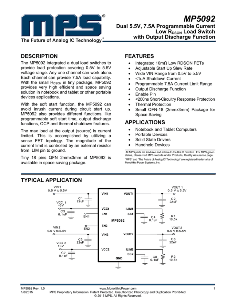
TYPICAL APPLICATION
MP5092 Rev. 1.0
1/8/2015
www.MonolithicPower.com
MPS Proprietary Information. Patent Protected. Unauthorized Photocopy and Duplication Prohibited.
© 2015 MPS. All Rights Reserved.
1
MP5092 – DUAL 5.5V, 7.5A LOW RDSON LOAD SWITCH WITH OUTPUT DISCHARGE FUNCTION
ORDERING INFORMATION
Part Number*
MP5092GD
Package
QFN-18 (2mmx3mm)
Top Marking
See Below
* For Tape & Reel, add suffix –Z (e.g. MP5092GD–Z);
TOP MARKING
AKF: product code of MP5092GD;
Y: year code;
LLL: lot number;
PACKAGE REFERENCE
TOP VIEW
QFN-18 (2mmx3mm)
MP5092 Rev. 1.0
1/8/2015
www.MonolithicPower.com
MPS Proprietary Information. Patent Protected. Unauthorized Photocopy and Duplication Prohibited.
© 2015 MPS. All Rights Reserved.
2
MP5092 – DUAL 5.5V, 7.5A LOW RDSON LOAD SWITCH WITH OUTPUT DISCHARGE FUNCTION
ABSOLUTE MAXIMUM RATINGS (1)
Thermal Resistance
VIN1/2 .......................................... –0.3V to +6.5V
VCC1/2 ......................................... –0.3V to +6.5V
VOUT1/2 ........................................ –0.3V to +6.5V
All Other Pins .......................–0.3V to Vcc+0.3 V
Junction Temperature .............................. 150°C
Lead Temperature ................................... 260°C
(2)
Continuous Power Dissipation
QFN18 (2mmx3mm) ..................................1.8W
QFN-18 (2mmx3mm) ……....…70
Recommended Operating Conditions
(3)
Supply Voltage VIN1/2 ...................... 0.5V to 5.5V
Supply Voltage VCC1/2 ........................ 3V to 5.5V
Output Voltage VOUT1/2.................... 0.5V to 5.5V
Operating Junction Temp. (TJ). -40°C to +125°C
MP5092 Rev. 1.0
1/8/2015
(4)
θJA
θJC
15
°C/W
Notes:
1) Exceeding these ratings may damage the device.
2) The maximum allowable power dissipation is a function of the
maximum junction temperature TJ (MAX), the junction-toambient thermal resistance θJA, and the ambient temperature
TA. The maximum allowable continuous power dissipation at
any ambient temperature is calculated by PD (MAX) = (TJ
(MAX)-TA)/θJA. Exceeding the maximum allowable power
dissipation will cause excessive die temperature, and the
regulator will go into thermal shutdown. Internal thermal
shutdown circuitry protects the device from permanent
damage.
3) The device is not guaranteed to function outside of its
operating conditions.
4) Measured on JESD51-7, 4-layer PCB.
www.MonolithicPower.com
MPS Proprietary Information. Patent Protected. Unauthorized Photocopy and Duplication Prohibited.
© 2015 MPS. All Rights Reserved.
3
MP5092 – DUAL 5.5V, 7.5A LOW RDSON LOAD SWITCH WITH OUTPUT DISCHARGE FUNCTION
ELECTRICAL CHARACTERISTICS
VIN = 3.6V, VCC = 3.6V, TA = 25°C, unless otherwise noted.
Parameters
Input and Supply Voltage Range
Input Voltage
Supply Voltage
Supply Current (Single Channel)
Off State Leakage Current
VCC Standby Current
Symbol
VIN
VCC
IOFF
ISTBY
Power FET
ON Resistance
Condition
RDSON
Min
Typ
0.5
3
VIN=5V, EN=0
Max
Units
5.5
5.5
V
V
1
µA
1
330
µA
VCC=5V, EN=0
VCC=5V, Enable, No load
0.1
220
VCC=5.0V
VCC=3.3V
10
12
mΩ
155
30
°C
°C
Thermal Shutdown and Recovery
(5)
Shutdown Temperature
TSTD
(5)
Hysteresis
THYS
Under/Over Voltage Protection (Single Channel)
VCC Under Voltage Lockout
VCC_UVLO UVLO Rising Threshold
Threshold
UVLO Hysteresis
VUVLOHYS
Soft Start
SS pull-up current
ISS
Fixed slew rate
Enable
EN Rising Threshold
VENH
EN Hysteresis
VENHYS
ILIM
RLIM=10.5kΩ, rise Io,
(5)
Current limit
IOUT
record its peak value
(6)
Current Limit Accuracy
RLIM=50kΩ
Discharge Resistance (Single Channel)
Resistance
RDIS
2.6
1.3
2.8
200
mV
9
µA
1.5
400
1.7
7.5
1.54
V
1.64
200
V
mV
A
1.74
A
Ω
Notes:
5) Guarantee by characterization -Not production tested.
6) If sense current is smaller than 1.5A, the accuracy will be affected by some internal offset.
MP5092 Rev. 1.0
1/8/2015
www.MonolithicPower.com
MPS Proprietary Information. Patent Protected. Unauthorized Photocopy and Duplication Prohibited.
© 2015 MPS. All Rights Reserved.
4
MP5092 – DUAL 5.5V, 7.5A LOW RDSON LOAD SWITCH WITH OUTPUT DISCHARGE FUNCTION
TYPICAL PERFORMANCE CHARACTERISTICS
VIN = 3.6V, VCC = 3.6V, RLIM=10.5k, TA = 25°C, unless otherwise noted.
300
300
250
250
200
200
150
150
100
100
50
50
0
0
-50
2.5
3 3.5
4 4.5
5 5.5
6 6.5
0.5
0.45
0.4
0.35
0.3
0.25
0.2
-50
0
50
100
150
0.6
0.4
0.2
0
-0.2
-0.4
-0.6
-0.8
0
50
100
150
-1
1.8
1.8
1.6
1.6
1.4
1.4
1.2
1.2
1
1
0.8
0.8
0.6
0.6
0.4
0.4
0.2
0.2
0
-50
14
16
12
14
0
50
100
150
2
0
-50
3
4
5
6
0
50
100
150
60
50
12
10
40
10
8
8
6
30
6
4
4
2
2
0
2.5
1
0.8
3 3.5
MP5092 Rev. 1.0
1/8/2015
4 4.5
5 5.5
6 6.5
0
-50
20
10
0
50
100
150
0
0
1
2
3
4
www.MonolithicPower.com
MPS Proprietary Information. Patent Protected. Unauthorized Photocopy and Duplication Prohibited.
© 2015 MPS. All Rights Reserved.
5
6
7
8
9
5
MP5092 – DUAL 5.5V, 7.5A LOW RDSON LOAD SWITCH WITH OUTPUT DISCHARGE FUNCTION
TYPICAL PERFORMANCE CHARACTERISTICS (continued)
VIN = 3.6V, VCC = 3.6V, RLIM=10.5k, TA = 25°C, unless otherwise noted.
8
40
100000
7
35
10000
6
5
30
25
1000
4
20
100
3
2
MP5092 Rev. 1.0
1/8/2015
10
10
1
0
-40 -20
15
1
0
20
40
60
80 100
5
1
10
100
1000
0
0
1
2
3
4
www.MonolithicPower.com
MPS Proprietary Information. Patent Protected. Unauthorized Photocopy and Duplication Prohibited.
© 2015 MPS. All Rights Reserved.
5
6
7
8
9
6
MP5092 – DUAL 5.5V, 7.5A LOW RDSON LOAD SWITCH WITH OUTPUT DISCHARGE FUNCTION
TYPICAL PERFORMANCE CHARACTERISTICS (continued)
VIN = 3.6V, VCC = 3.6V, RLIM=10.5k, TA = 25°C, unless otherwise noted.
Enable Startup
Enable Startup
Enable Shutdown
VIN =3.6V, VCC=3.6V, No Load
VIN =3.6V, VCC=3.6V, 7A Load
VIN =3.6V, VCC=3.6V, No Load
VOUT
2V/div.
VEN
5V/div.
VOUT
2V/div.
VEN
5V/div.
VOUT
2V/div.
VEN
5V/div.
ILIM
500mV/div.
ILIM
500mV/div.
ILIM
500mV/div.
IOUT
5A/div.
IOUT
5A/div.
IOUT
5A/div.
Enable Shutdown
Enable Startup
Enable Startup
VIN =3.6V, VCC=3.6V, 7A Load
VIN=1.8V, VCC=3.6V, No Load
VIN=1.8V, VCC=3.6V, 7A Load
VOUT
2V/div.
VEN
5V/div.
VOUT
1V/div.
VEN
5V/div.
VOUT
1V/div.
VEN
5V/div.
ILIM
500mV/div.
ILIM
500mV/div.
ILIM
500mV/div.
IOUT
5A/div.
IOUT
5A/div.
IOUT
5A/div.
Enable Shutdown
Enable Shutdown
Enable Startup
VIN=1.8V, VCC=3.6V,No Load
VIN=1.8V, VCC=3.6V, 7A Load
VIN=1.1V, VCC=3.6V, No Load
VOUT
1V/div.
VEN
5V/div.
VOUT
1V/div.
VEN
5V/div.
VOUT
1V/div.
VEN
5V/div.
ILIM
500mV/div.
ILIM
500mV/div.
ILIM
500mV/div.
IOUT
5A/div.
IOUT
5A/div.
IOUT
5A/div.
MP5092 Rev. 1.0
1/8/2015
www.MonolithicPower.com
MPS Proprietary Information. Patent Protected. Unauthorized Photocopy and Duplication Prohibited.
© 2015 MPS. All Rights Reserved.
7
MP5092 – DUAL 5.5V, 7.5A LOW RDSON LOAD SWITCH WITH OUTPUT DISCHARGE FUNCTION
TYPICAL PERFORMANCE CHARACTERISTICS (continued)
VIN = 3.6V, VCC = 3.6V, RLIM=10.5k, TA = 25°C, unless otherwise noted.
Enable Startup
Enable Shutdown
Enable Shutdown
VIN=1.1V, VCC=3.6V, 7A Load
VIN=1.1V, VCC=3.6V, No Load
VIN=1.1V, VCC=3.6V, 7A Load
VOUT
1V/div.
VEN
5V/div.
VOUT
1V/div.
VEN
5V/div.
VOUT
1V/div.
VEN
5V/div.
ILIM
500mV/div.
ILIM
500mV/div.
ILIM
500mV/div.
IOUT
5A/div.
IOUT
5A/div.
IOUT
5A/div.
Power Up
Power Up
VIN =3.6V, VCC=3.6V, No Load
VIN =3.6V, VCC=3.6V, 7A Load
Power Down
VIN =3.6V, VCC=3.6V, No Load
VOUT
2V/div.
VIN
2V/div.
VOUT
2V/div.
VIN
2V/div.
VOUT
2V/div.
VIN
2V/div.
ILIM
500mV/div.
ILIM
500mV/div.
ILIM
500mV/div.
IOUT
5A/div.
IOUT
5A/div.
IOUT
5A/div.
Power Down
Steady State
VIN =3.6V, VCC=3.6V, 7A Load
VIN =3.6V, VCC=3.6V, 7A Load
VOUT
2V/div.
VIN
2V/div.
VOUT
2V/div.
VIN
2V/div.
ILIM
500mV/div.
ILIM
500mV/div.
IOUT
5A/div.
IOUT
5A/div.
MP5092 Rev. 1.0
1/8/2015
Load Transient Response
VIN =5V, VCC=3.3V, IOUT=0A to 7A
VOUT
2V/div.
VIN
5V/div.
IOUT
5A/div.
www.MonolithicPower.com
MPS Proprietary Information. Patent Protected. Unauthorized Photocopy and Duplication Prohibited.
© 2015 MPS. All Rights Reserved.
8
MP5092 – DUAL 5.5V, 7.5A LOW RDSON LOAD SWITCH WITH OUTPUT DISCHARGE FUNCTION
TYPICAL PERFORMANCE CHARACTERISTICS (continued)
VIN = 3.6V, VCC = 3.6V, RLIM=10.5k, TA = 25°C, unless otherwise noted.
SCP Entery
SCP Steady State
VIN =5V, VCC=3.3V, RLIM=10.5k
VIN =5V, VCC=3.3V, RLIM=10.5k
SCP Recovery
VIN =5V, VCC=3.3V, RLIM=10.5k
VOUT
2V/div.
VOUT
2V/div.
VOUT
2V/div.
VIN
5V/div.
VIN
5V/div.
VIN
5V/div.
IOUT
5A/div.
IOUT
5A/div.
IOUT
5A/div.
MP5092 Rev. 1.0
1/8/2015
www.MonolithicPower.com
MPS Proprietary Information. Patent Protected. Unauthorized Photocopy and Duplication Prohibited.
© 2015 MPS. All Rights Reserved.
9
MP5092 – DUAL 5.5V, 7.5A LOW RDSON LOAD SWITCH WITH OUTPUT DISCHARGE FUNCTION
PIN FUNCTIONS
(2x3)QFN18
Pin #
Name
1, 13
2, 12
3, 11
VIN1
VOUT1
VOUT2
4, 10
VIN2
5
EN2
6, 15
7
GND
VCC2
8
ILIM2
9
SS2
14
EN1
16
VCC1
17
ILIM1
18
SS1
MP5092 Rev. 1.0
1/8/2015
Description
Input Power Supply of Switch 1.
Output to the Load of Switch 1.
Output to the Load of Switch 2.
Input Power Supply of Switch 2.
Enable Input of Switch 2. Pulling this pin below the specified threshold shuts the
chip down.
Ground.
Switch 2’s Supply Voltage to the Control Circuitry.
Output Current Limit Configure of Switch 2. Place a resistor to ground to set the
overload current limit level.
Soft start control pin of load Switch 2. Connecting a capacitor from this pin to
ground to set the soft start time.
Enable Input of Switch 1. Pulling this pin below the specified threshold shuts the
chip down.
Switch 1’s Supply Voltage to the Control Circuitry.
Output Current Limit Configure of Switch 1. Place a resistor to ground to set the
overload current limit level.
Soft Start Control Pin of Load Switch 1. Connecting a capacitor from this pin to
ground to set the soft start time.
www.MonolithicPower.com
MPS Proprietary Information. Patent Protected. Unauthorized Photocopy and Duplication Prohibited.
© 2015 MPS. All Rights Reserved.
10
MP5092 – DUAL 5.5V, 7.5A LOW RDSON LOAD SWITCH WITH OUTPUT DISCHARGE FUNCTION
BLOCK DIAGRAM
VIN1
Charge
Pump
Current
Sense
VCC
4
ILIM1
VOUT1
Fast Off Comp
Soft Start
1V
Current Limit Amp
SS1
UVLO
VCC
Control Logic
EN1
4
8
Thermal
Sense
80
GND
VCC1
Figure 1: Functional Block Diagram
(Only Channel 1 Included, Channel 2 is the same)
MP5092 Rev. 1.0
1/8/2015
www.MonolithicPower.com
MPS Proprietary Information. Patent Protected. Unauthorized Photocopy and Duplication Prohibited.
© 2015 MPS. All Rights Reserved.
11
MP5092 – DUAL 5.5V, 7.5A LOW RDSON LOAD SWITCH WITH OUTPUT DISCHARGE FUNCTION
OPERATION
The MP5092 is designed to limit the in-rush
current to the load when a circuit card is
inserted into a live backplane power source;
thereby limiting the backplane’s voltage drop
and the slew rate of the voltage to the load.
MP5092 integrated two independent load
switches. Any one channel can work alone.
Each channel can provide 7.5A load capability.
It provides an integrated solution to monitor
output current to eliminate the need for an
external current power MOSFET, and current
sense device.
Enable
When input voltage is greater than the undervoltage lockout threshold (UVLO), typically 0.5V,
MP5092 can be enabled by pulling EN pin to
higher than 1.5V. Pulling down to ground will
disable MP5092.
The recommend start up sequence is power up
VIN first. After VIN is ready, pull EN voltage to
high.
Current Limit
The MP5092 provides a constant current limit
that can be programmed by an external resistor.
Once the device reaches its current limit
threshold, the internal circuit regulates the gate
voltage to hold the current in the power FET
constant. The typical response time is about
20µs and the output current may have a small
overshoot during this time period.
The pre-set current limit value
calculated by below equation:
ILIM ( A ) =
82000
R LIM (Ω)
can
be
(1)
RLIM is R1 and R2 which are placed between
ILIM1/2 pin to ground in Figure 4.
If the current limit block starts to regulate the
output current, the power loss on power
MOSFET will cause the IC temperature rise. If
the junction temperature rose to high enough, it
will trigger thermal shutdown. After thermal
shutdown happened, it will disable the output
until the over temperature fault remove. The
MP5092 Rev. 1.0
1/8/2015
over temperature threshold is 155oC and
hysteresis is 30oC.Bias Vcc Supply
Vcc is the bias supply for internal analog circuit.
It is better to have a decouple capacitor to filter
the noise. If the main power voltage VIN is
higher than 3V, the Vcc can be directly
connected to VIN.
Short-Circuit Protection
If the load current increases rapidly due to a
short circuit, the current may exceed the current
limit threshold by a lot before the control loop
can respond. If the current reaches an internal
secondary current limit level (about 13A), a fast
turn-off circuit activates to turn off the power
FET. This limits the peak current through the
switch to limit the input voltage drop. The total
short circuit response time is about 200ns. If
fast off works, it will keep off the power FET for
80us. After that time period, it will re-turn on
power FET..
Output Discharge
MP5092 has output discharge function. This
function can discharge the Vo by internal pull
down resistance when IC disabled and the load
is very light.
Soft-Start
A capacitor connected to the SS pin determines
the soft-start time. There is an internal 9uA
constant current source charge SS cap and
ramps up the voltage on the SS pin. The output
voltage rises at 3 times the slew rate to the SS
voltage.
The soft-start time can be calculated by below
equation:
TSS (ms) =
1 VOUT ( V ) ⋅ C SS (nF)
×
(2)
3
ISS (uA )
TSS is the soft-start time, ISS is internal 9uA
constant current, CSS is external soft-start cap.
The suggestion minimum SS cap should be
bigger than 4.7nF. If the SS pin is floated or SS
cap is too small, the Vo rising time will be just
limited by power MOS charge time.
www.MonolithicPower.com
MPS Proprietary Information. Patent Protected. Unauthorized Photocopy and Duplication Prohibited.
© 2015 MPS. All Rights Reserved.
12
MP5092 – DUAL 5.5V, 7.5A LOW RDSON LOAD SWITCH WITH OUTPUT DISCHARGE FUNCTION
APPLICATION INFORMATION
ILIM Resistor Selection
The current limit value can be set by ILIM
resistor. The current limit can be gotten by
equation (1).
The current limit threshold is suggested to 10%
~ 20% higher than maximum load current. For
example, if the system’s full load is 7A, set the
current limit to 7.7A.
ILIM Capacitor Selection
The internal advanced auto-zero comparator
bring a high accuracy of current limit. The autozero will also cause some little jitter on ILIM pin.
To get a more stable ILIM, a small ceramic
capacitor can be mounted between ILIM and
ground. Suggested place a ILIM capacitor less
than 1nF.
Soft Start Capacitor Selection
There is an internal 9uA constant current
source charge SS cap and ramps up the
voltage on the SS pin. The output voltage rises
follow 3 times the slew rate of SS voltage.
If the inrush on output current reached the
current limit during start up (like with large
output cap or very large load), MP5092 will limit
the output current and the same time, SS time
will be increased (Figure 2).
MP5092 Rev. 1.0
1/8/2015
Soft Start @ Different Output Capacitance
VOUT
Current Limit
IIN
Soft Start @ Small Capacitance
VOUT
Current Limit
IIN
Soft Start @ Large Capacitance
VOUT
Current Limit
IIN
Soft Start @ Very large
Capacitance
Figure 2: Soft Start Periods at different output
capacitance
www.MonolithicPower.com
MPS Proprietary Information. Patent Protected. Unauthorized Photocopy and Duplication Prohibited.
© 2015 MPS. All Rights Reserved.
13
MP5092 – DUAL 5.5V, 7.5A LOW RDSON LOAD SWITCH WITH OUTPUT DISCHARGE FUNCTION
Design Example
Some design examples are provided below.
See Table 1 and Figure 3.
Table 1
VIN
(V)
5
5
5
Current limit
(A)
3
5
7.5
RLIM
(kΩ)
26.1
15.8
10.5
SS cap
(nF)
22
47
100
SS time
(ms)
4
9
20
Figure 3: Typical Application Schematic
Layout Guide
PCB layout is very important to achieve stable
operation. Please follow these guidelines and
take below figure for reference (take schematic
in Figure 3 as an example). Place ILIM resistor
(R1 and R2 in Figure 3) close to ILIM1/2 pin,
input cap close to VCC pin. Put enough vias
around IC to achieve better thermal
performance.
Figure 4: Recommended Layout
MP5092 Rev. 1.0
1/8/2015
www.MonolithicPower.com
MPS Proprietary Information. Patent Protected. Unauthorized Photocopy and Duplication Prohibited.
© 2015 MPS. All Rights Reserved.
14
MP5092 – DUAL 5.5V, 7.5A LOW RDSON LOAD SWITCH WITH OUTPUT DISCHARGE FUNCTION
PACKAGE INFORMATION
QFN18 (2mmx3mm)
PIN 1 ID
MARKING
PIN 1 ID
0.15X0.10 TYP
PIN 1 ID
INDEX AREA
TOP VIEW
BOTTOM VIEW
SIDE VIEW
NOTE:
0.15X0.10
1) ALL DIMENSIONS ARE IN MILLIMETERS.
2) EXPOSED PADDLE SIZE DOES NOT
INCLUDE MOLD FLASH.
3) LEAD COPLANARITY SHALL BE 0.10
MILLIMETERS MAX.
4) JEDEC REFERENCE IS MO-220.
5) DRAWING IS NOT TO SCALE.
RECOMMENDED LAND PATTERN
NOTICE: The information in this document is subject to change without notice. Please contact MPS for current specifications.
Users should warrant and guarantee that third party Intellectual Property rights are not infringed upon when integrating MPS
products into any application. MPS will not assume any legal responsibility for any said applications.
MP5092 Rev. 1.0
1/8/2015
www.MonolithicPower.com
MPS Proprietary Information. Patent Protected. Unauthorized Photocopy and Duplication Prohibited.
© 2015 MPS. All Rights Reserved.
15
