Gate Drive Optocoupler Basic Design for IGBT / MOSFET
Applicable to All Gate Drive Optocouplers
Application Note 5336
Introduction
IGBT/MOSFET Gate Resistor
This application note covers the topic of calculating gate
driver power and thermal dissipation of the gate drive
optocoupler IC. Gate drive optocouplers are used to
drive, turning-on and off, power semiconductor switches,
MOSFETs / IGBTs. The gate drive power calculation can be
divided into three parts; power consumed or lost in the
internal circuitry of the driver, power sent to the power
semiconductor switches (IGBT/MOSFET) and power lost
at the external component between the driver IC and the
power semiconductor switch, e.g. across external gate
resistor. In the following example, we will discuss an IGBT
gate driver design using the Avago ACPL-332J (2.5nApeak
intelligent gate driver). This design guide is applicable for
MOSFET gate drivers also.
When choosing the value of RG, it is important to look
from the point from both gate driver IC and the power
semiconductor switches, MOSFET/IGBT. For the gate
driver IC, we choose an RG that is within the IC maximum
allowable power disippation rating while sourcing/
sinking the highest possible driver current. From the IGBT
or MOSFET point of view, the gate resistor influences the
voltage change dVCE/dt and current change diC/dt during
the turn on and turn off period.
So it is important when a designer chooses an IGBT or
MOSFET, the appropriate gate driver optocoupler is also
chosen as the current and power rating of this driver
determine how fast the IGBT or MOSFETcan turn on or
turn off.
13
VCC2
UVLO
ANODE
CATHODE
6, 7
D
R
I
V
E
R
5, 8
LED1
11
14
DESAT
9, 12
SHIELD
VOUT
DESAT
VEE
VCLAMP
VCC1
FAULT
VS
2
3
10
LED2
16
1, 4
15
SHIELD
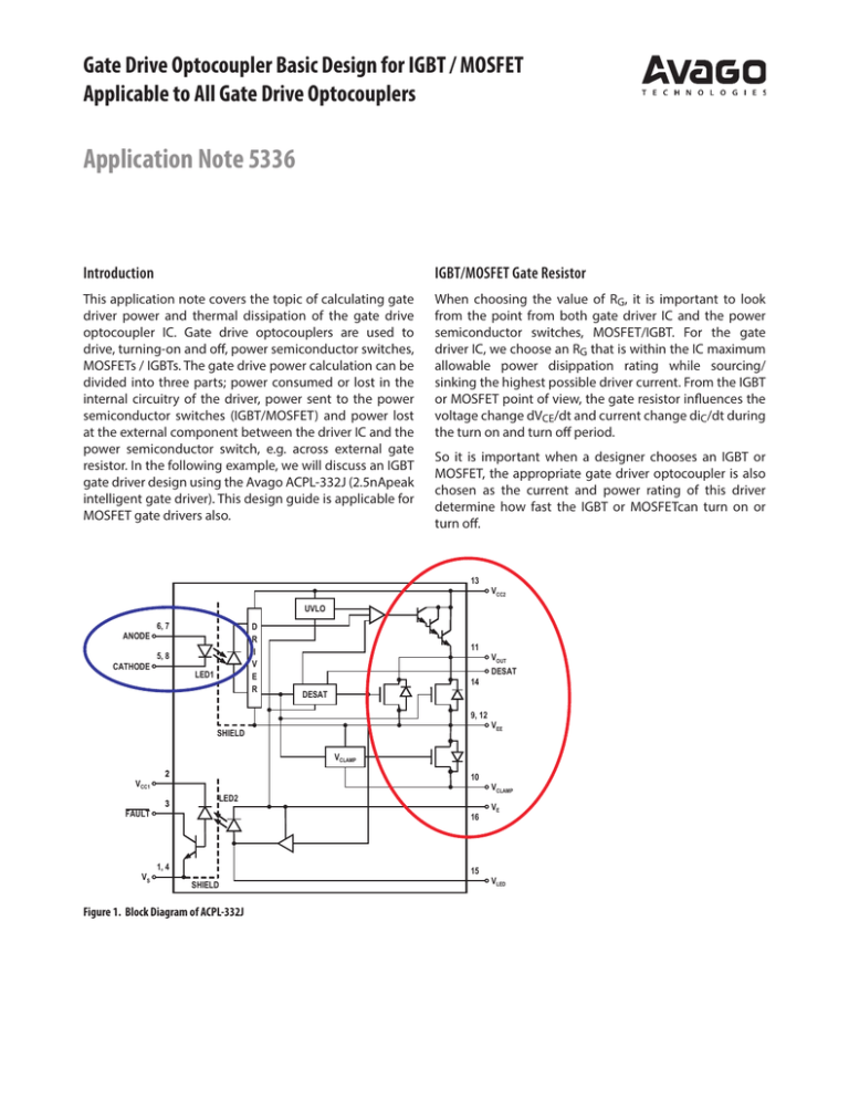
Figure 1. Block Diagram of ACPL-332J
VCLAMP
VE
VLED
Gate Drive Power Operation within IC Maximum Allowable
Power Ratings
The power dissipation of the gate drive optocoupler is a
combination of output-side power to the IGBT/MOSFET,
red circle, and the input-side power due to input LED
power dissipation, blue circle. The power dissipation for
the second LED used for fault feedback is neglected as
the current to drive the open-collector transistor is small.
The calculation steps are:
1.Calculate the minimum desired RG according to the
maximum peak gate current
2. Calculate total power dissipation
3.Compare the input and output power dissipation
calculated in step #2 to the maximum recommended
dissipation for the IC. (If the maximum recommended
level has been exceeded, it may be necessary to raise
the value of RG to lower the switching power and
repeat step #2.)
In this example, the total input and output power dissipation of the ACPL-332J is calculated given the following
conditions:
Rg= (VCC2 – VEE – VOL)/ IOL = (18 V - (-5 V) - 6.3)/ 2.5 A
= 6.68 Ω (approximately 6.8 Ω)
Note: The value of the gate resistance has a significant
impact on the dynamic performance of IGBTs/MOSFETs.
A smaller gate resistor charges and discharges the power
transistor input capacitance faster, reducing switching
times and switching losses. The trade off is that this could
lead to higher voltage oscillations. In the MOSFET and
IGBT datasheet, there is usually a recommended gate
resistor which is used for the datasheet characterization.
However, a designer should be cautious not to over-drive
the gate drive IC by using the recommended gate resistance from the IGBT or MOSFET datasheet.
Step II: Calculate total power dissipation in the gate driver:
The total power dissipation (PT ) is equal to the sum of the
input-side power (PI) and output-side power (PO) dissipation:
PT = PI + PO
•IG = ION, MAX ~ 2.5 A
PI = IF(ON) ,max * VF,max
• VCC2 = 18 V
where,
• VEE = -5 V, (Note: VEE = 0 V if negative voltage supply is
not required in application)
• fSWITCH = 15 kHz
IF(ON),max = 12 mA
VF,max = 1.95 V
The IF(ON) can be found in the recommended operting
conditions and VF can be found in the ACPL-332J datasheet, Table 5 of the electrical specifications.
• Ambient Temperature = 70° C
Step I: Calculate RG minimum from IOL peak specification:
To find the peak charging lOL assume that the gate is
initially charged to the steady-state value VCC. For the
ACPL-332J, the voltage drop is linearly approximated as
6.3 V for 2.5 A output at 70° C (Fig 2: VOL vs IOL). Therefore
apply the following relationship:
Electrical Specification
Input Forward Voltage, VF
Min
Typ
Max
Units
1.2
1.6
1.95
V
PO= PO(BIAS) + PO(SWTICH)
VOL - LOW OUTPUT VOLTAGE DROP - V
= ICC2.MAX * (VCC2–VEE ) + ∆VGE * QG * fSWITCH
8
where,
_ _ _ _ 100 o C
______ 25 o C
--------- -40 o C
7
6
PO(BIAS)
PO(SWITCH) = Driver power for charging and discharging
of device gate capacitances.
5
4
ICC2.MAX =Supply current to power internal circuity
3
2
1
0
0
0.5
1
1.5
IoL - OUTPUT LOW CURRENT - A
Figure 2. VOL vs IOL
2
=Steady-state power in the driver due to
biasing the device.
2
∆VGE =VCC2 + |VEE|
QG =Total gate charge of the IGBT or MOSFET
as described in the manufacturer specification (Illustrated in Figure 3) = 240 nC
(approximation for a 100 A IGBT)
fSWITCH =Switching frequency of application
2.5
Using the above information, we calculate both PI and PO
below:
The output detector junction temperature is given by:
PI = 12 mA * 1.95 V = 23.4 mW
Using the qJ-P = q9-12 = 30° C/W (ACPL-332J Table 7,
Package Characteristic) and a TA of 70° C and assuming
the thermal resistance from pin to ambient, qP-A is
50° C/W:
PO = PO(BIAS) + PO(SWITCH)
= 5.0 mA * (18 V – (–5 V)) + (18 V + 5 V) * 240nC * 15 kHz
= 115 mW + 82.8 mW
TJ = PD *( qJ-P + qP-A) + TA
TJ = 197.8*(30+50) + 70° C = 85.8° C
= 197.8 mW
If the juntion temperature is higher than the maximum
junction temperature rating (in this case 125° C), the
desired specification must be derated according.
VGE(V)
+VGE (VCC2)
Designers should note that the thermal resistance
between pin to ambient is also the PCB heatsink thermal
resistance. This thermal resistance is then dependent on
the area on the PCB and the free air-flow.
Further Topics:
QG(C)
-VGE (VEE)
QG
Figure 3. Typical IGBT Gate Charge Curve
Step III: Compare the calculated power dissipation with the
absolute maximum values in the IC:
For the ACPL-332J, the maximum power dissipation can
be found in Table 3 of the ACPL-332J data sheet. Also, it
requires a derating of 10 mW/°C if the operating temperature is above 90° C (Note. 2 ACPL-332J datasheet).
Absolute Maximum Rating
Min
Max
Units
Output IC Power Dissipataion, Po
600
mW
Input IC Power Dissipation, PI
150
PI = 23.4 mW < 150 mW (abs. max.) ) OK
PO = 197.8 mW < 600 mW (abs. max.) ) OK
Therefore, the power dissipation absolute maximum
rating has not been exceeded for the above example.
Note: Heat dissipation for different packages require derating when
the operating temperature exceed a certain level. For ACPL-332J,
as operating temperature is below 90° C, derating is not necessary.
Operating temperature is different for different products
Another method to check if the device is within the
maximum limits is to calculate the junction temperature
of the device. We continue to use the example provided
earlier.
Power dissipation, PD = 23.4 + 197.8 = 221.2 mW
Higher Output Current Using an External Current Buffer:
To increase the IGBT gate drive current, a non-inverting
current buffer (such as the NPN/PNP buffer shown in
Figure 75 of HCPL-316J data sheet) may be used. Inverting
types are not compatible with the desatura-tion fault
protection circuitry and should be avoided. To preserve
the slow IGBT turn-off feature during a fault condition,
a 10 nF capacitor should be connected from the buffer
input to VEE and a 10 Ω resistor inserted between the
output and the common NPN/PNP base. The MJD44H11/
MJD45H11 pair is appropriate for currents up to 8 A
maximum. The D44VH10/ D45VH10 pair is appropriate
for currents up to 15 A maximum.
Thermal Model
Most of the steady state thermal models for gate drive
optocouplers can be found in AN1087. The thermal resistance values given in this model can be used to calculate
the temperatures at each node for a given operating
condition.
HCPL-316J
VE
16
VLED2+
15
DESAT
14
VCC2
13
VC
12
VOUT
11
VEE
10
VEE
9
100 pF
MJD44H11 or
D44VH10
4.5 Ω
10 Ω
2.5 Ω
10 nF
MJD45H11 or
D45VH10
15 V
-5 V
Figure 4. Current Buffer for Increased Drive Current
3
Printed Circuit Board Layout Considerations
Adequate spacing should always be maintained between
the high voltage isolated circuitry and any input referenced circuitry. Care must be taken to provide the same
minimum spacing between two adjacent high-side
isolated regions of the printed circuit board. Insufficient
spacing will reduce the effective isolation and increase
parasitic coupling that will degrade CMR performance.
The placement and routing of supply bypass capacitors
requires special attention. During switching transients,
the majority of the gate charge is supplied by the bypass
capacitors. Maintaining short bypass capacitor trace
lengths will ensure low supply ripple and clean switching
waveforms.
Figure 5 below shows an example PCB layout using the
HCPL-316J gate driver optocoupler. Ground Plane con-
nections are necessary for pin 4 (GND1) and pins 9 and
10 (VEE) in order to achieve maximum power dissipation
as the HCPL-316J is designed to dissipate the majority
of heat generated through these pins. This is also applicable for the ACPL-332J. For this case, the ground plane
connections are pin 1, pin 4 (VSS) and pin 4 (VSS), pin 9
and 12 (VEE). Actual power dissipation will depend on
the application environment (PCB layout, air flow, part
placement, etc.) See Application Note 1087 or details on
how to estimate junction temperature.
The layout examples in Figure 5 have good supply
bypassing and thermal properties, exhibit small PCB footprints, and have easily connected signal and supply lines.
The four examples cover single sided and double sided
component placement, as well as minimal and improved
performance circuits.
Figure 5. Recommended layout(s)
For product information and a complete list of distributors, please go to our web site:
www.avagotech.com
Avago, Avago Technologies, and the A logo are trademarks of Avago Technologies in the United States and other countries.
Data subject to change. Copyright © 2005-2014 Avago Technologies. All rights reserved.
AV02-0421EN - February 25, 2014


