USB 2.0 PCB Guidelines for the
ArcticLink® Solution Platform
••••••
QuickLogic® Application Note 93
Introduction
This document provides guidelines for component placement and PCB routing of the USB 2.0 portion of the
QuickLogic ArcticLink solution platform. Follow the suggested guidelines to minimize signal integrity issues.
Overview
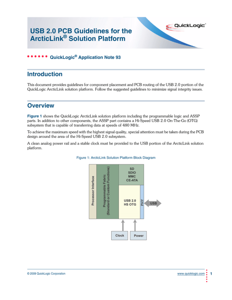
Figure 1 shows the QuickLogic ArcticLink solution platform including the programmable logic and ASSP
parts. In addition to other components, the ASSP part contains a Hi-Speed USB 2.0 On-The-Go (OTG)
subsystem that is capable of transferring data at speeds of 480 MHz.
To achieve the maximum speed with the highest signal quality, special attention must be taken during the PCB
design around the area of the Hi-Speed USB 2.0 subsystem.
A clean analog power rail and a stable clock must be provided to the USB portion of the ArcticLink solution
platform.
SD
SDIO
MMC
CE-ATA
USB 2.0
HS OTG
Clock
CLOCK
PHY
Programmable Fabric
(Standard or Custom Functions)
Processor Interface
Figure 1: ArcticLink Solution Platform Block Diagram
USB
USB
Power
POWER
•
© 2009 QuickLogic Corporation
www.quicklogic.com ••
•
•
•
1
USB 2.0 PCB Guidelines for the ArcticLink® Solution Platform Rev. C
USB OTG Schematic
Figure 2 shows an electrical schematic of the USB OTG area and the component locations relative to each
other:
• USB Subsystem
• Power Supply
• Reference Resistor
• Connector
Figure 2: USB OTG Schematic
U1
J1
VDDA
VBUS
VDDA
C1
C2
100 nF
1 nF
ArticLink
VDDP
100 nF
1 nF
2
3
4
ID
1
USB
2
VSSP
3
REFEXT
5.9 K
1%
OTG_ CL K
R1
FB2
U2
AGND
AGND
1
DP
VSSA
VDDP
C4
F-BEAD
DM
AGND
C3
FB1
AGND
I/O1
I/O4
GND
VBUS
I/O2
I/O3
F-BEAD
5
6
6
5
4
C5
100 nF
C6
100 nF
7
8
9
USBLC6-4SC6
C7
C8
VBUS
DD+
ID
GND
CHASSIS
CHASSIS
CHASSIS
CHASSIS
100 nF
440479-1
USB OTG PO RT (TYPE A/B)
100 nF
AGND
12 MHz
DGND
AGND
USB Subsystem
The USB subsystem is comprised of the following components:
• U1- ArcticLink solution platform USB subsystem.
• U2– ESD protection device (e.g., USBLC6-4SC6).
• FB1 and FB2 Ferrite Beads – For cleaning the power line of the externally connected USB device.
• C5,C6,C7, and C8 – Capacitor 100 nF – Decoupling caps for the USB connector.
Power Supply
The power supply for the USB OTG area is comprised of the following components:
• C1 and C2 – Decoupling capacitor 100 nF (ceramic X7R).
• C3 and C4 – Decoupling capacitor (e.g., 1 nF, ceramic X7R) – Analog power rail decoupling caps for the
ArcticLink solution platform. Two values are used to cover a wider spectral range.
•
2 •• www.quicklogic.com
•
•
•
© 2009 QuickLogic Corporation
USB 2.0 PCB Guidelines for the ArcticLink® Solution Platform Rev. C
Reference Resistor
The reference resistor for the USB OTG area is:
• R1 – Resistor 5.9 KΩ (to 1%) – OTG external reference resistor.
Connector
The connector for the USB OTG area is:
• J1 – USB OTG connector (Type A, mini-AB, etc.).
NOTE: Analog and digital ground must be connected on the board at one place only to level potentials and
to avoid noise crossing.
Component Placement
The design of the PCB layout requires careful placement of the components as follows:
1. Place the USB OTG connector (J1) on the board.
2. Place the ArcticLink solution platform (U1) on the board no further than 2 to 3 inches from the USB OTG
connector.
Leave space for ESD protection device (U2) and decoupling components (i.e., C1, C2, etc.).
For easier PCB routing, make sure to correctly rotate the ArcticLink solution platform.
The USB signals on the ArcticLink solution platform are placed at the edge of the package.
Place the ferrite beads (FB1 and FB2) close to USB OTG connector (J1).
3. Place the power-decoupling capacitors close to the ArcticLink solution platform (U1) or USB OTG
connector (J1).
The lower value capacitors must be placed closer to the components.
Stack-Up Recommendation
The ArcticLink solution platform can be routed in six layers. To route the ArcticLink solution platform in
six layers, QuickLogic recommends the following stack-up:
• Layer 1 – Top layer for components and high-speed signals
• Layer 2 – Power plane - GND
• Layer 3 – Inner signal layer routing
• Layer 4 – Inner signal layer routing
• Layer 5 – Power plane – VCC (split between different voltages)
• Layer 6 – Bottom layer for signal routing and passive components
•
© 2009 QuickLogic Corporation
www.quicklogic.com ••
•
•
•
3
USB 2.0 PCB Guidelines for the ArcticLink® Solution Platform Rev. C
If Hi-Speed USB signals are routed on the top layer, best results will be obtained if Layer 2 is a ground plane.
Furthermore, there must be only one ground plane under the Hi-Speed USB signals in order to keep the HiSpeed USB signals from crossing another ground plane. Figure 3 shows examples of correct and incorrect
power plane configurations on the layer below the top layer DP and DM signals.
Figure 3: Power Plane Configurations
DM
Layer 1 - Top layer,
signal and components
DP
dielectic
Layer 2 - GND plane
GND
Correct – Layout with USB signals over compact ground plane.
DM
Layer 1 - Top layer,
signal and components
DP
dielectic
Layer 2 - GND plane
GND1
GND2
Incorrect – Layout with USB signals over split ground plane.
PCB Design Layout Suggestions
To minimize signal integrity issues, follow these PCB design layout suggestions:
1. Route the DP and the DM signals first. To gain the 90 Ω differential impedance, use a dielectric thickness
of 4 mils, a trace spacing and a trace width of 7.5 mils to 8 mils.
NOTE: Differential impedance can be controlled by the trace width, the trace spacing and the dielectric
thickness.
2. Route the DP and DM signals between the ArcticLink solution platform and the USB OTG connector, and
through the ESD device on the top layer, keeping the length difference less than 150 mils. Try to route the
signals less than 5 inches in length. Avoid the creation of stubs on these lines. If a stub is unavoidable in
the design, stubs must not be longer than 200 mils.
3. Route the power decoupling with thick trace to connect to the power plane.
4. Route the clock lines. Create the clock lines as short as possible with a low capacitance line (5 mils
thickness) on the top layer.
•
4 •• www.quicklogic.com
•
•
•
© 2009 QuickLogic Corporation
USB 2.0 PCB Guidelines for the ArcticLink® Solution Platform Rev. C
5. Route high-speed signals far from the clock line (a minimum of 50 mils distance) to reduce crystal jitter.
6. Route the ferrite beads with thick trace (15 mils is the minimum recommended).
Figure 4 shows an example of data USB line routing, where the DP and DM signals are parallel.
Figure 4: Recommended Trace Width and Spacing
Top View
b
ArcticLink
b
b
USB
Connector
Trace width and
spacing equal to "b"
Side View
Low Speed
Signals
DP
3b
b
High Speed
and Clock
Signals
DM
b
b
7b
Conclusion
This application note covers component placement PCB routing for the QuickLogic ArcticLink solution
platform. Follow the recommendations in this application note to get the optimum signal quality on the USB
bus and to minimize problems related to signal integrity. For more references or the latest version of this
application note visit the QuickLogic website at www.quicklogic.com.
•
© 2009 QuickLogic Corporation
www.quicklogic.com ••
•
•
•
5
USB 2.0 PCB Guidelines for the ArcticLink® Solution Platform Rev. C
Contact Information
Phone: (408) 990-4000 (US)
(905) 940-4149 (Canada)
+(44) 1932-57-9011 (Europe)
+(852) 2567-5441 (Asia)
E-mail:
info@quicklogic.com
Sales:
America-sales@quicklogic.com
Europe-sales@quicklogic.com
Asia-sales@quicklogic.com
Japan-sales@quicklogic.com
Support: www.quicklogic.com/support
Internet: www.quicklogic.com
Revision History
Revision
Date
A
April 2007
B
November 2008
C
April 2008
Originator and Comments
First release
Vasuki Uttamalingam and Elaine Chan
Kathleen Murchek
Updated contact and trademark info.
Added Notice of Disclaimer.
Kathleen Murchek
Updated trademark info..
Notice of Disclaimer
QuickLogic is providing this design, product or intellectual property "as is." By providing the design, product or intellectual property as
one possible implementation of your desired system-level feature, application, or standard, QuickLogic makes no representation that this
implementation is free from any claims of infringement and any implied warranties of merchantability or fitness for a particular purpose.
You are responsible for obtaining any rights you may require for your system implementation. QuickLogic shall not be liable for any
damages arising out of or in connection with the use of the design, product or intellectual property including liability for lost profit, business
interruption, or any other damages whatsoever. QuickLogic products are not designed for use in life-support equipment or applications
that would cause a life-threatening situation if any such products failed. Do not use QuickLogic products in these types of equipment or
applications.
QuickLogic does not assume any liability for errors which may appear in this document. However, QuickLogic attempts to notify
customers of such errors. QuickLogic retains the right to make changes to either the documentation, specification, or product without
notice. Verify with QuickLogic that you have the latest specifications before finalizing a product design.
•
6 •• www.quicklogic.com
•
•
•
© 2009 QuickLogic Corporation
USB 2.0 PCB Guidelines for the ArcticLink® Solution Platform Rev. C
Copyright and Trademark Information
Copyright © 2009 QuickLogic Corporation. All Rights Reserved.
The information contained in this document is protected by copyright. All rights are reserved by QuickLogic Corporation. QuickLogic
Corporation reserves the right to modify this document without any obligation to notify any person or entity of such revision. Copying,
duplicating, selling, or otherwise distributing any part of this product without the prior written consent of an authorized representative of
QuickLogic is prohibited.
QuickLogic and ArcticLink are registered trademarks of QuickLogic Corporation; the QuickLogic logo are trademarks of QuickLogic.
Other trademarks are the property of their respective companies.
•
© 2009 QuickLogic Corporation
www.quicklogic.com ••
•
•
•
7
