EIE4401
advertisement
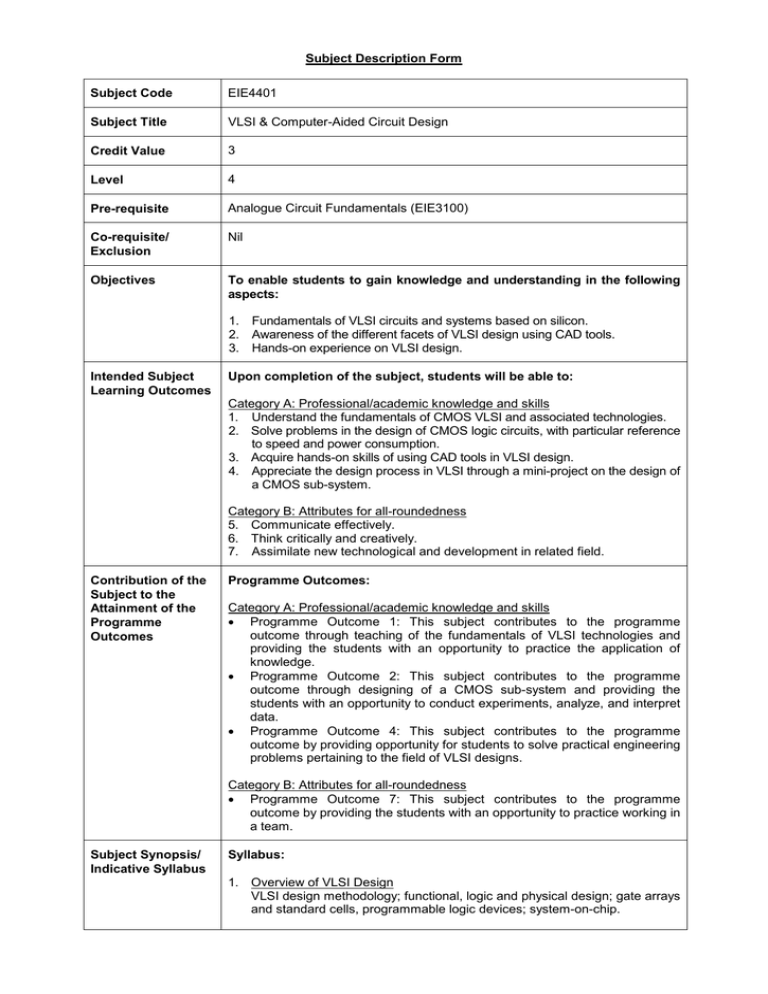
Subject Description Form Subject Code EIE4401 Subject Title VLSI & Computer-Aided Circuit Design Credit Value 3 Level 4 Pre-requisite Analogue Circuit Fundamentals (EIE3100) Co-requisite/ Exclusion Nil Objectives To enable students to gain knowledge and understanding in the following aspects: 1. Fundamentals of VLSI circuits and systems based on silicon. 2. Awareness of the different facets of VLSI design using CAD tools. 3. Hands-on experience on VLSI design. Intended Subject Learning Outcomes Upon completion of the subject, students will be able to: Category A: Professional/academic knowledge and skills 1. Understand the fundamentals of CMOS VLSI and associated technologies. 2. Solve problems in the design of CMOS logic circuits, with particular reference to speed and power consumption. 3. Acquire hands-on skills of using CAD tools in VLSI design. 4. Appreciate the design process in VLSI through a mini-project on the design of a CMOS sub-system. Category B: Attributes for all-roundedness 5. Communicate effectively. 6. Think critically and creatively. 7. Assimilate new technological and development in related field. Contribution of the Subject to the Attainment of the Programme Outcomes Programme Outcomes: Category A: Professional/academic knowledge and skills • Programme Outcome 1: This subject contributes to the programme outcome through teaching of the fundamentals of VLSI technologies and providing the students with an opportunity to practice the application of knowledge. • Programme Outcome 2: This subject contributes to the programme outcome through designing of a CMOS sub-system and providing the students with an opportunity to conduct experiments, analyze, and interpret data. • Programme Outcome 4: This subject contributes to the programme outcome by providing opportunity for students to solve practical engineering problems pertaining to the field of VLSI designs. Category B: Attributes for all-roundedness • Programme Outcome 7: This subject contributes to the programme outcome by providing the students with an opportunity to practice working in a team. Subject Synopsis/ Indicative Syllabus Syllabus: 1. Overview of VLSI Design VLSI design methodology; functional, logic and physical design; gate arrays and standard cells, programmable logic devices; system-on-chip. 2. CMOS Fabrication and Layout Fabrication processes in CMOS VLSI; latch-up; characteristics of devices in VLSI; mask layout techniques and design rules. 3. CMOS Logic Circuits Transmission gates; static and dynamic gates and flip flops; domino logic; low power design; design for testability. 4. High Speed CMOS Logic Design Delay estimation and transistor sizing; device and interconnect capacitance; optimal delay design of buffers; power supply grid; clock distribution. 5. CAD Techniques in VLSI Design Circuit and logic simulation, mask layout, layout extraction and verification; standard cell placement and routing. 6. Sub-system Design Examples to illustrate sub-system design in VLSI: data path in a microprocessor, random-access-memory. Laboratory Experiment: 1. Practice of CAD tools for VLSI design: circuit simulation, mask layout, layout extraction and verification, placement and routing. 2. Mini-project: design of a sub-system for computer or communication applications. Teaching/ Learning Methodology Teaching and Learning Method Intended Subject Learning Outcome Remarks Lectures, supplemented with interactive questions and answers, and short quizzes 1, 2, 6, 7 In lectures, students are introduced to the and knowledge of the subject, comprehension is strengthened with interactive Q&A and short quizzes. They will be able to explain and generalize knowledge in VLSI. Tutorials where design problems are discussed, and are given to students for them to solve 1, 2, 5, 6 In tutorials, students apply what they have learnt in analyzing the cases and solving the problems given by the tutor. They will analyze the given information, compare and contrast different scenarios and propose solutions or alternatives. Laboratory sessions, where students will perform a miniproject on a subsystem design using CAD tools. They will have to write a report on their mini-projects. 2, 3, 4, 5, 6 Students acquire hands-on experience in using CAD tools in VLSI design, and apply what they have learnt in lectures/tutorials to do a mini-project on the design of a sub-system. Assignment and Homework 1, 2, 3, 4, 5, 6 Through working assignment and homework, students will develop a firm understanding and comprehension of the knowledge taught. They will analyze given information and apply knowledge in solving problem. For some design type of questions, they will have to synthesize solutions by alternatives. Alignment of Assessment and Intended Subject Learning Outcomes Specific Assessment Methods/Tasks % Weighting evaluating different Intended Subject Learning Outcomes to be Assessed (Please tick as appropriate) 1 2 3 4 5 6 1. Continuous Assessment (total 50%) • Assignment/Homework/ Case study reports 10% • Laboratory works and reports 30% • Mid-semester test 5% • End-of-semester test 5% 2. Examination 50% Total 100% The continuous assessment will consist of a mini-project, a number of assignments, and two tests. Explanation of the appropriateness of the assessment methods in assessing the intended learning outcomes: Specific Assessment Methods/ Tasks Remark Assignment/ Homework/Case study reports Assignment/Homework and case study reports are given to students to assess their competence level of knowledge and comprehension, ability to analyze given information, ability to apply knowledge and skills in new situation, ability to synthesize structure, and ability to evaluate given data to make judgment. The criteria (i.e. what to be demonstrated) and level (i.e. the extent) of achievement will be graded according to six levels: (A+ and A), Good (B+ and B), Satisfactory (C+ and C), Marginal (D) and Failure (F). These will be made known to the students before an assignment/homework is given. Feedback about their performance will be given promptly to students to help them improvement their learning. Laboratory works and reports Students will be required to perform a mini-project and submit a report. The emphasis is on assessing their ability to use VLSI CAD tools effectively to perform VLSI design. Expectation and grading criteria will be given as in the case of assignment/homework. Mid-semester test There will be a mid-semester test to evaluate students’ achievement of all the learning outcomes and give feedback to them for prompt improvement. Expectation and grading criteria will be given as in the case of assignment/homework. End-of-semester test and There will be an end-of-semester test and examination to assess students’ achievement of all Examination Student Study Effort Expected the learning outcomes. These are mainly summative in nature. Expectation and grading criteria will be given as in the case of assignment/homework. Class contact (time-tabled): • Lecture 24 Hours • Tutorial/Laboratory/Practice Classes 18 hours Other student study effort: • Lecture: preview/review of notes; homework/assignment; preparation for test/quizzes/examination 36 Hours • Tutorial/Laboratory/Practice Classes: preview of materials, revision and/or reports writing 27 Hours Total student study effort: Reading List and References 105 Hours Reference Books: 1. N.H.E. Weste and D. Harris, CMOS VLSI Design – A Circuits and Systems rd Perspective, 3 ed., Reading: Addison-Wesley, 2005. st 2. M.M. Vai, VLSI Design, 1 ed., Boca Raton: CRC Press, 2001. 3. D.A. Hodges, H.G. Jackson and R.A. Saleh, Analysis and Design of Digital rd Integrated Circuits, 3 ed., New York: McGraw-Hill, 2003. rd 4. W. Wolf, Modern VLSI Design: System-on-chip Design, 3 ed., Englewood Cliffs: Prentice-Hall, 2002. Last Updated Aug 2012 Prepared by Dr Martin Chow
