CMOS Layout Minimization via Euler's Path Rule
advertisement

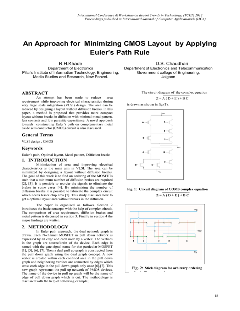
International Conference & Workshop on Recent Trends in Technology, (TCET) 2012 Proceedings published in International Journal of Computer Applications® (IJCA) An Approach for Minimizing CMOS Layout by Applying Euler’s Path Rule R.H.Khade Department of Electronics Pillai’s Institute of Information Technology, Engineering, Media Studies and Research, New Panvel. ABSTRACT An attempt has been made to reduce area requirement while improving electrical characteristics during very large scale integration (VLSI) design. The area can be reduced by designing a layout without diffusion breaks. In this paper, a method is proposed that provides more compact layout without breaks in diffusion with minimal metal pattern, less contacts and low parasitic capacitance. A novel approach towards constructing Euler’s path on complementary metal oxide semiconductor (CMOS) circuit is also discussed. D.S. Chaudhari Department of Electronics and Telecommunication Government college of Engineering, Jalgaon The circuit diagram of the complex equation Z=A(D+E)+BC is drawn as shown in fig (1). General Terms VLSI design , CMOS Keywords Euler’s path, Optimal layout, Metal pattern, Diffusion breaks 1. INTRODUCTION Minimization of area and improving electrical characteristics is the main aim in VLSI. The area can be minimized by designing a layout without diffusion breaks. The goal of this work is to find an ordering of the MOSFETs such that a minimum number of diffusion brakes are required [2], [3]. It is possible to reorder the signals to eliminate the brakes in some cases [4]. By minimizing the number of diffusion breaks it is possible to fabricate the complex circuit which needs lesser chip area [7]. This study discusses how to get a optimal layout area without breaks in the diffusion. Fig. 1: Circuit diagram of COMS complex equation Z=A(D+E)+BC The paper is organized as follows. Section 2 introduces the basic concepts with the help of complex circuit. The comparison of area requirement, diffusion brakes and metal pattern is discussed in section 3. Finally in section 4 the major findings are written. 2. METHODOLOGY In Euler path approach, the dual network graph is drawn. Each N-channel MOSFET in pull down network is expressed by an edge and each node by a vertex. The vertices in the graph are source/drain of the device. Each edge is named with the gate signal name for that particular MOSFET [1], [5], [6], [7]. Then a dual pull up graph is constructed from the pull down graph using the dual graph concept. A new vertex is created within each confined area in the pull down graph and neighboring vertices are connected by edges which cross each edge in the pull down graph only once [6],[7]. This new graph represents the pull up network of PMOS devices. The name of the device in pull up graph will be the name of edge of pull down graph which is cut. The methodology is discussed with the help of following example; Stick diagram for arbitrary ordering of polysilicon gate columns. 18 International Conference & Workshop on Recent Trends in Technology, (TCET) 2012 Proceedings published in International Journal of Computer Applications® (IJCA) The Euler graph of fig (1) network is as shown in fig.(3) VOUT B VOUT A B A VOUT VDD E D E D C C Gnd VSS Fig. 3: Euler graph VOUT B The separated pull down and pull up graphs are shown in fig.(4) and fig.(5) A VOUT B A E D C E D VSS C VSS Fig. 4: NMOS Graph VDD The Euler path in the pull down graph and pull up graph with identical ordering of input labels are drawn as shown in fig (4) and (5). The Euler path is defined as an uninterrupted path that traverses each edge (branch) of the graph exactly once. To simplify the metal connections following rules are used: For pull down D i) ii) If only one source is connected to Vss then start from extreme left. iii) If two sources are connected to Vss then start the metal pattern of Vss connection in between two polysilicon strips or two metal strips at two ends of diffusion. iv) If three sources are connected to Vss then one Vss connection from extreme left which will connect the source to ground and other two sources are connected by drawing metal strip from Vss and between two polysilicon strips of the two devices whose sources are to be connected to Vss. E A C B For pull down start from Vss/Vout. VOUT Fig. 5: PMOS Graph For pull down i) ii) For pull up start from VDD/Vout. If only one source of PMOS device is connected to VDD then draw metal strip from extreme left. 19 International Conference & Workshop on Recent Trends in Technology, (TCET) 2012 Proceedings published in International Journal of Computer Applications® (IJCA) iii) iv) If two sources are connected to VDD then start the metal pattern of VDD connection between two polysilicon strips or two metal strips at two ends of diffusion.. 3. RESULT AND DISCUSSION The mask layout for arbitrary ordering of polysilicon gates is shown in fig (7). Fig(8) shows proposed layout when Euler’s rules are used. If three sources are connected to VDD then one VDD connection from extreme left which will connect source of one device to VDD and other two sources are connected by drawing metal strip from VDD and between two polysilicon strip of the two devices whose sources are to be connected to VDD. If odd number (N) of sources are connected to ground / VDD then total vertical metal strips from VSS/VDD to diffusion (if there are no breaks in diffusion) will be 1 + (N−1)/2 One metal strip from extreme end and (N-1)/2 will be between polysilicon strips. The number of vertical metal strips from VSS/VDD to diffusion will be minimum if there are no breaks in diffusion. If breaks in diffusion are present then some extra metal strips from VSS/VDD to diffusion are required, which will increase area and parasitic capacitance If even number of sources (N) are connected to V SS/VDD then total vertical metal strips from VSS/VDD to diffusion will be, Length = 75 2 + (N−2)/2 ( if two metal strips are at extreme ends of diffusion.) or Fig. 7: Mask layout for arbitrary ordering of polysilicon gate columns. N/2 (if no metal strips at extreme ends of diffusion.) While drawing metal strips from VSS/VDD , follow the path and name the terminals of the device. The stick diagram of fig (1) using Euler’s rule is shown in fig.(6) VDD Vout D E C B A VSS Fig. 6: Stick Diagram for polysilicon ordering using Euler’s rules. The names of terminals of the devices are given according to the path travelled. Length = 57 Fig. 8: Mask layout for polysilicon gate column ordering using Euler’s rules. From the two layouts drawn using Microwind software following observations regarding area of the layouts, diffusion breaks and number of metal contacts are made. 20 International Conference & Workshop on Recent Trends in Technology, (TCET) 2012 Proceedings published in International Journal of Computer Applications® (IJCA) Parameter Layout for arbitrary ordering of polysilicon gate columns. Proposed layout using Euler’s rule. Length 75 57 Diffusion breaks 4 Nil Metal contacts at diffusion 16 10 Table 1 The layout comparisons are shown in Table (1), it is clear that the length required using proposed method is less as compared to the length required using arbitrary ordering of polysilicon gate column method. Due to reduction in length less area is required. For the example discussed above, there is 24% saving in the area. The diffusion breaks and metal contacts at diffusion are reduced in the proposed method. Due to this the parasitic capacitance decreases which helps in reduction of the propagation delay time. 4. CONCLUSION This work changes the viewpoint of ordering of polysilicon gate columns and constructing the metal pattern on CMOS circuits and puts some basic layout ideas into systematic approach. The method makes more compact layout with less breaks in diffusion, metal contacts and parasitic capacitance. The proposed method provides another way of designing metal pattern using Euler’s path on CMOS circuits. REFERENCES [1] Shun-wen Cheng, Kou-Hsing Cneng. 2004. “Modified Euler path Rule for MOS Layout Minimization. ”, in IEEE Asia-Pacific Conference on Circuits and Systems, pp, 541-544, December 6-9, 2004 [2] Shaoan Yan, Dongen Li, Liming Wang, Yongguang Xiao, Minghua Tang. “A Novel Methodology of Layout Design by applying Euler path”, .10th IEEE International Conference on Solid-State and Integrated Circuit Technology (ICSICT),2010 [3] Y.J. Kwon and C.M. Kyung, “An Algorithm for optimal layouts of CMOS complex logic Modules“, in Proc. IEEE International Symposium on Circuits and Systems, vol.5, pp. 3126-3129, June 1991. [4] T. Nakagaki, S. Yamada and K.Fukunaga, “ Fast Optimal Algorithm for the CMOS Functional Cell Layout Based on Transistor Reordering,” in Proc. IEEE International Symposium Circuits and System, vol.5, pp, 2116-2119, May 1992. [5] N.H.E. Weste , K. Eshraghian, Principle of CMOS VLSI Design. 2nd Edition, Reading : Addison-wesley, 1993. [6] John P. Uyemura, Introduction to VLSI circuits and Systems, John Wiley & Sons, p.80,2002.. [7] Sung-Mo Kang, Yusuf Leblebici, CMOS Digital Integrated Circuits, Analysis and Design, 3rd Edition, Tata McGraw- Hill Edition, 2003. 21

