Phase-Locked Loops for High-Frequency
advertisement

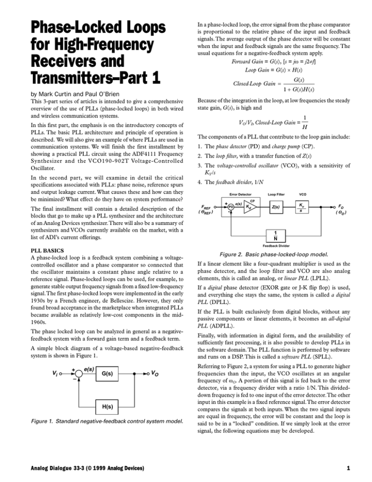
Phase-Locked Loops for High-Frequency Receivers and Transmitters–Part 1 In a phase-locked loop, the error signal from the phase comparator is proportional to the relative phase of the input and feedback signals. The average output of the phase detector will be constant when the input and feedback signals are the same frequency. The usual equations for a negative-feedback system apply. Forward Gain = G(s), [s = jω = j2πf] Loop Gain = G(s) × H(s) Closed−Loop Gain = by Mark Curtin and Paul O’Brien This 3-part series of articles is intended to give a comprehensive overview of the use of PLLs (phase-locked loops) in both wired and wireless communication systems. In this first part, the emphasis is on the introductory concepts of PLLs. The basic PLL architecture and principle of operation is described. We will also give an example of where PLLs are used in communication systems. We will finish the first installment by showing a practical PLL circuit using the ADF4111 Frequency Synthesizer and the VCO190-902T Voltage-Controlled Oscillator. In the second part, we will examine in detail the critical specifications associated with PLLs: phase noise, reference spurs and output leakage current. What causes these and how can they be minimized? What effect do they have on system performance? The final installment will contain a detailed description of the blocks that go to make up a PLL synthesizer and the architecture of an Analog Devices synthesizer. There will also be a summary of synthesizers and VCOs currently available on the market, with a list of ADI’s current offerings. G(s) 1 + G(s)H(s) Because of the integration in the loop, at low frequencies the steady state gain, G(s), is high and VO /VI, Closed-Loop Gain = 1 H The components of a PLL that contribute to the loop gain include: 1. The phase detector (PD) and charge pump (CP). 2. The loop filter, with a transfer function of Z(s) 3. The voltage-controlled oscillator (VCO), with a sensitivity of KV /s 4. The feedback divider, 1/N Error Detector FREF ( UREF ) + PD - e(s) Loop Filter VCO CP Kd Z(s) Kv s FO ( UO ) 1 N Feedback Divider PLL BASICS A phase-locked loop is a feedback system combining a voltagecontrolled oscillator and a phase comparator so connected that the oscillator maintains a constant phase angle relative to a reference signal. Phase-locked loops can be used, for example, to generate stable output frequency signals from a fixed low-frequency signal. The first phase-locked loops were implemented in the early 1930s by a French engineer, de Bellescize. However, they only found broad acceptance in the marketplace when integrated PLLs became available as relatively low-cost components in the mid1960s. The phase locked loop can be analyzed in general as a negativefeedback system with a forward gain term and a feedback term. A simple block diagram of a voltage-based negative-feedback system is shown in Figure 1. Vi + – e(s) G(s) VO H(s) Figure 1. Standard negative-feedback control system model. Analog Dialogue 33-3 (© 1999 Analog Devices) Figure 2. Basic phase-locked-loop model. If a linear element like a four-quadrant multiplier is used as the phase detector, and the loop filter and VCO are also analog elements, this is called an analog, or linear PLL (LPLL). If a digital phase detector (EXOR gate or J-K flip flop) is used, and everything else stays the same, the system is called a digital PLL (DPLL). If the PLL is built exclusively from digital blocks, without any passive components or linear elements, it becomes an all-digital PLL (ADPLL). Finally, with information in digital form, and the availability of sufficiently fast processing, it is also possible to develop PLLs in the software domain. The PLL function is performed by software and runs on a DSP. This is called a software PLL (SPLL). Referring to Figure 2, a system for using a PLL to generate higher frequencies than the input, the VCO oscillates at an angular frequency of ωO. A portion of this signal is fed back to the error detector, via a frequency divider with a ratio 1/N. This divideddown frequency is fed to one input of the error detector. The other input in this example is a fixed reference signal. The error detector compares the signals at both inputs. When the two signal inputs are equal in frequency, the error will be constant and the loop is said to be in a “locked” condition. If we simply look at the error signal, the following equations may be developed. 1 () e s = Φ REF − ()=F de s REF ΦO When GH is much greater than 1, we can say that the closed loop transfer function for the PLL system is N and so N FOUT = N × FREF − dt FO The loop filter is a low-pass type, typically with one pole and one zero. The transient response of the loop depends on: N When 1. the magnitude of the pole/zero, () e s = constant , FO 2. the charge pump magnitude, = FREF 3. the VCO sensitivity, N Thus 4. the feedback factor, N. FO = N FREF VCO Output Frequency (MHz) In commercial PLLs, the phase detector and charge pump together form the error detector block.When FO ≠ N FREF, the error detector will output source/sink current pulses to the low-pass loop filter. This smooths the current pulses into a voltage which in turn drives the VCO. The VCO frequency will then increase or decrease as necessary, by KV DV, where KV is the VCO sensitivity in MHz/ Volt and DV is the change in VCO input voltage. This will continue until e(s) is zero and the loop is locked. The charge pump and VCO thus serves as an integrator, seeking to increase or decrease its output frequency to the value required so as to restore its input (from the phase detector) to zero. ∆F KV = ∆F/∆V ∆V VCO Tuning Voltage (Volts) Figure 3. VCO transfer function. The overall transfer function (CLG or Closed-Loop Gain) of the PLL can be expressed simply by using the CLG expression for a negative feedback system as given above. FO = FREF Forward Gain The phase-locked loop allows stable high frequencies to be generated from a low-frequency reference. Any system that requires stable high frequency tuning can benefit from the PLL technique. Examples of these applications include wireless base stations, wireless handsets, pagers, CATV systems, clock-recovery and -generation systems. A good example of a PLL application is a GSM handset or base station. Figure 4 shows the receive section of a GSM base station. In the GSM system, there are 124 channels (8 users per channel) of 200-kHz width in the RF band. The total bandwidth occupied is 24.8 MHz, which must be scanned for activity. The handset has a transmit (Tx) range of 880 MHz to 915 MHz and a receive (Rx) range of 925 MHz to 960 MHz. Conversely, the base station has a Tx range of 925 MHz to 960 MHz and an Rx range of 880 MHz to 915 MHz. For this example, we will consider just the base station transmit and receive sections. The frequency bands for GSM900 and DCS1800 Base Station Systems are shown in Table 1. Table 2 shows the channel numbers for the carrier frequencies (RF channels) within the frequency bands of Table 1. Fl(n) is the center frequency of the RF channel in the lower band (Rx) and Fu(n) is the corresponding frequency in the upper band (Tx). () TX K D KV Z s P-GSM900 DCS1800 E-GSM900 s Loop Gain , GH = PLL APPLICATIONS TO FREQUENCY UPSCALING Table 1. Frequency Bands for GSM900 and DCS1800 Base Station Systems 1 + Loop Gain Forward Gain , G = All of the above must be taken into account when designing the loop filter. In addition, the filter must be designed to be stable (usually a phase margin of π/4 is recommended). The 3-dB cutoff frequency of the response is usually called the loop bandwidth, BW. Large loop bandwidths result in very fast transient response. However, this is not always advantageous, as we shall see in Part 2, since there is a tradeoff between fast transient response and reference spur attenuation. () K D KV Z s RX 935 to 960 MHz 1805 to 1880 MHz 925 to 960 MHz 890 to 915 MHz 1710 to 1785 MHz 880 to 915 MHz Ns Table 2. Channel Numbering for GSM900 and DCS1800 Base Station Systems RX 2 TX PGSM900 Fl(n) = 890 + 0.2 × (n) 1 ≤ n ≤ 124 Fu(n) = Fl(n) + 45 EGSM900 Fl(n) = 890 + 0.2 × (n) Fl(n) = 890 + 0.2 × (n – 1024) 0 ≤ n ≤ 124 975 ≤ n ≤ 1023 Fu(n) = Fl(n) + 45 DCS1800 Fl(n) = 1710.2 + 0.2 × (n – 512) 512 ≤ n ≤ 885 Fu(n) = Fl(n) + 95 Analog Dialogue 33-3 (© 1999 Analog Devices) 900MHz RF -104dBm to 60dBm TCXO 13MHz VCO Synthesizer Synthesizer VCO 640MHz to 675MHz 229.3MHz L0 1 Tuned 1ST IF 240 MHz L0 2 Fixed 2ND IF 10.7 MHz Demodulator Figure 4. Signal chain for GMS base-station receiver. The 900-MHz RF input is filtered, amplified and applied to the first stage mixer. The other mixer input is driven from a tuned local oscillator (LO). This must scan the input frequency range to search for activity on any of the channels. The actual implementation of the LO is by means of the PLL technique already described. If the 1st intermediate-frequency (IF) stage is centered at 240 MHz, then the LO must have a range of 640 MHz to 675 MHz in order to cover the RF input band. When a 200-kHz reference frequency is chosen, it will be possible to sequence the VCO output through the full frequency range in steps of 200 kHz. For example, when an output frequency of 650 MHz is desired, N will have a value of 3250. This 650-MHz LO will effectively check the 890MHz RF channel (FRF – FLO = FIF or FRF = FLO + FIF). When N is incremented to 3251, the LO frequency will now be 650.2 MHz and the RF channel checked will be 890.2 MHz. This is shown graphically in Figure 5. GSM Example (N-1)FREF (N)FREF (N+1)FREF ∆F = FREF For GSM: FREF = 200 kHz FRF = 880MHz to 915MHz for the Receiver If First IF is at 240MHz then LO must go from 640MHz to 675MHz. This Means N must vary from 3200 to 3375 Figure 5. Testing frequencies for GSM base-station receiver. Analog Dialogue 33-3 (© 1999 Analog Devices) It is worth noting that, in addition to the tunable RF LO, the receiver section also uses a fixed IF (in the example shown this is 240 MHz). Even though frequency tuning is not needed on this IF, the PLL technique is still used. The reason for this is that it is an affordable way of using the stable system reference frequency to produce the high frequency IF signal. Several synthesizer manufacturers recognize this fact by offering dual versions of the devices: one operating at the high RF frequency (>800 MHz) and one operating at the lower IF frequency (500 MHz or less). On the transmit side of the GSM system, similar requirements exist. However, it is more common to go directly from baseband to the final RF in the Transmit section; this means that the typical TX VCO for a base station has a range of 925 MHz to 960 MHz (RF band for the Transmit section). CIRCUIT EXAMPLE Figure 6 shows an actual implementation of the local oscillator for the transmit section of a GSM handset. We are assuming direct baseband to RF up-conversion. This circuit uses the new ADF4111 PLL Frequency Synthesizer from ADI and the VCO190-902T Voltage Controlled Oscillator from Vari-L Corporation (http:// www.vari-L.com/). The reference input signal is applied to the circuit at FREFIN and is terminated in 50 Ω. This reference input frequency is typically 13 MHz in a GSM system. In order to have a channel spacing of 200 kHz (the GSM standard), the reference input must be divided by 65, using the on-chip reference divider of the ADF4111. The ADF4111 is an integer-N PLL frequency synthesizer, capable of operating up to an RF frequency of 1.2 GHz. In this integer-N type of synthesizer, N can be programmed from 96 to 262,000 in discrete integer steps. In the case of the handset transmitter, where an output range of 880 MHz to 915 MHz is needed, and where the internal reference frequency is 200 kHz, the desired N values will range from 4400 to 4575. 3 The charge pump output of the ADF4111 (Pin 2) drives the loop filter. This filter (Z(s) in Figure 2) is basically a 1st-order lag-lead type. In calculating the loop filter component values, a number of items need to be considered. In this example, the loop filter was designed so that the overall phase margin for the system would be 45 degrees. Other PLL system specifications are given below: KD = 5 mA KV = 8.66 MHz/V Loop Bandwidth = 12 kHz FREF = 200 kHz N = 4500 Extra Reference Spur Attenuation = 10 dB The ADF4111 uses a simple 4-wire serial interface to communicate with the system controller. The reference counter, the N counter and various other on-chip functions are programmed via this interface. CONCLUSION In this first part of the series, we have introduced the basic concepts of PLLs with simple block diagrams and equations. We have shown a typical example of where the PLL structure is used and given a detailed description of a practical implementation. In the next installment, we will delve deeper into the specifications which are critical to PLLs and discuss their system implications. All of these specifications are needed and used to come up with the loop filter components values shown in Figure 6. REFERENCES The loop filter output drives the VCO, which, in turn, is fed back to the RF input of the PLL synthesizer and also drives the RF Output terminal. A T-circuit configuration with 18-ohm resistors is used to provide 50-ohm matching between the VCO output, the RF output and the RFIN terminal of the ADF4111. 1. Mini-Circuits Corporation, “VCO Designers Handbook.” 2. L.W. Couch, “Digital and Analog Communications Systems” Macmillan Publishing Company, New York. 3. P. Vizmuller, “RF Design Guide,” Artech House. In a PLL system, it is important to know when the system is in lock. In Figure 6, this is accomplished by using the MUXOUT signal from the ADF4111. The MUXOUT pin can be programmed to monitor various internal signals in the synthesizer. One of these is the LD or lock-detect signal. When MUXOUT is chosen to select lock detect, it can be used in the system to trigger the output power amplifier, for example. VDD 4. R.L. Best, “Phase Locked Loops: Design, Simulation and Applications,” 3rd Edition, McGraw Hill. b VP RFOUT 100 pF 7 1000 pF 1000 pF 8 FREFIN 15 16 AVDD DVDD VP CP 14 3.3 kΩ 2 REFIN 5.6 kΩ 8.2 nF 14 3 MUXOUT 18 Ω 18 Ω 620 pF 1, 3, 4, 5, 7, 8, 9, 11, 12, 13 Lock Detect 100 pF RFINA 4 6 5 51 Ω DGND RFINB AGND CPGND CE CLK DATA LE 100 pF 18 Ω 10 VCO190-902T 1 nF ADF4111 51 Ω SPI Compatible Serial Bus 2 VCC 9 100 pF Decoupling Capacitors (0.1 µF/10 pF) on AVDD, DVDD, VP of the ADF4111 and on VCC of the VCO190-902T have been omitted from the diagram to aid clarity. Figure 6. Transmitter local oscillator for GSM handset. 4 Analog Dialogue 33-3 (© 1999 Analog Devices) 易迪拓培训 专注于微波、射频、天线设计人才的培养 网址:http://www.edatop.com 射 频 和 天 线 设 计 培 训 课 程 推 荐 易迪拓培训(www.edatop.com)由数名来自于研发第一线的资深工程师发起成立,致力并专注于微 波、射频、天线设计研发人才的培养;我们于 2006 年整合合并微波 EDA 网(www.mweda.com),现 已发展成为国内最大的微波射频和天线设计人才培养基地,成功推出多套微波射频以及天线设计经典 培训课程和 ADS、HFSS 等专业软件使用培训课程,广受客户好评;并先后与人民邮电出版社、电子 工业出版社合作出版了多本专业图书,帮助数万名工程师提升了专业技术能力。客户遍布中兴通讯、 研通高频、埃威航电、国人通信等多家国内知名公司,以及台湾工业技术研究院、永业科技、全一电 子等多家台湾地区企业。 易迪拓培训课程列表:http://www.edatop.com/peixun/rfe/129.html 射频工程师养成培训课程套装 该套装精选了射频专业基础培训课程、射频仿真设计培训课程和射频电 路测量培训课程三个类别共 30 门视频培训课程和 3 本图书教材;旨在 引领学员全面学习一个射频工程师需要熟悉、理解和掌握的专业知识和 研发设计能力。通过套装的学习,能够让学员完全达到和胜任一个合格 的射频工程师的要求… 课程网址:http://www.edatop.com/peixun/rfe/110.html ADS 学习培训课程套装 该套装是迄今国内最全面、最权威的 ADS 培训教程,共包含 10 门 ADS 学习培训课程。课程是由具有多年 ADS 使用经验的微波射频与通信系 统设计领域资深专家讲解,并多结合设计实例,由浅入深、详细而又 全面地讲解了 ADS 在微波射频电路设计、通信系统设计和电磁仿真设 计方面的内容。能让您在最短的时间内学会使用 ADS,迅速提升个人技 术能力,把 ADS 真正应用到实际研发工作中去,成为 ADS 设计专家... 课程网址: http://www.edatop.com/peixun/ads/13.html HFSS 学习培训课程套装 该套课程套装包含了本站全部 HFSS 培训课程,是迄今国内最全面、最 专业的 HFSS 培训教程套装,可以帮助您从零开始, 全面深入学习 HFSS 的各项功能和在多个方面的工程应用。购买套装,更可超值赠送 3 个月 免费学习答疑,随时解答您学习过程中遇到的棘手问题,让您的 HFSS 学习更加轻松顺畅… 课程网址:http://www.edatop.com/peixun/hfss/11.html ` 易迪拓培训 专注于微波、射频、天线设计人才的培养 网址:http://www.edatop.com CST 学习培训课程套装 该培训套装由易迪拓培训联合微波 EDA 网共同推出,是最全面、系统、 专业的 CST 微波工作室培训课程套装,所有课程都由经验丰富的专家授 课,视频教学,可以帮助您从零开始,全面系统地学习 CST 微波工作的 各项功能及其在微波射频、天线设计等领域的设计应用。且购买该套装, 还可超值赠送 3 个月免费学习答疑… 课程网址:http://www.edatop.com/peixun/cst/24.html HFSS 天线设计培训课程套装 套装包含 6 门视频课程和 1 本图书,课程从基础讲起,内容由浅入深, 理论介绍和实际操作讲解相结合,全面系统的讲解了 HFSS 天线设计的 全过程。是国内最全面、最专业的 HFSS 天线设计课程,可以帮助您快 速学习掌握如何使用 HFSS 设计天线,让天线设计不再难… 课程网址:http://www.edatop.com/peixun/hfss/122.html 13.56MHz NFC/RFID 线圈天线设计培训课程套装 套装包含 4 门视频培训课程,培训将 13.56MHz 线圈天线设计原理和仿 真设计实践相结合,全面系统地讲解了 13.56MHz 线圈天线的工作原理、 设计方法、设计考量以及使用 HFSS 和 CST 仿真分析线圈天线的具体 操作,同时还介绍了 13.56MHz 线圈天线匹配电路的设计和调试。通过 该套课程的学习,可以帮助您快速学习掌握 13.56MHz 线圈天线及其匹 配电路的原理、设计和调试… 详情浏览:http://www.edatop.com/peixun/antenna/116.html 我们的课程优势: ※ 成立于 2004 年,10 多年丰富的行业经验, ※ 一直致力并专注于微波射频和天线设计工程师的培养,更了解该行业对人才的要求 ※ 经验丰富的一线资深工程师讲授,结合实际工程案例,直观、实用、易学 联系我们: ※ 易迪拓培训官网:http://www.edatop.com ※ 微波 EDA 网:http://www.mweda.com ※ 官方淘宝店:http://shop36920890.taobao.com 专注于微波、射频、天线设计人才的培养 易迪拓培训 官方网址:http://www.edatop.com 淘宝网店:http://shop36920890.taobao.com


