SX1781
PLL Frequency Synthesizer with Integrated VCO
ADVANCED COMMUNICATIONS & SENSING
DATASHEET
FINAL
GENERAL DESCRIPTION
FEATURES
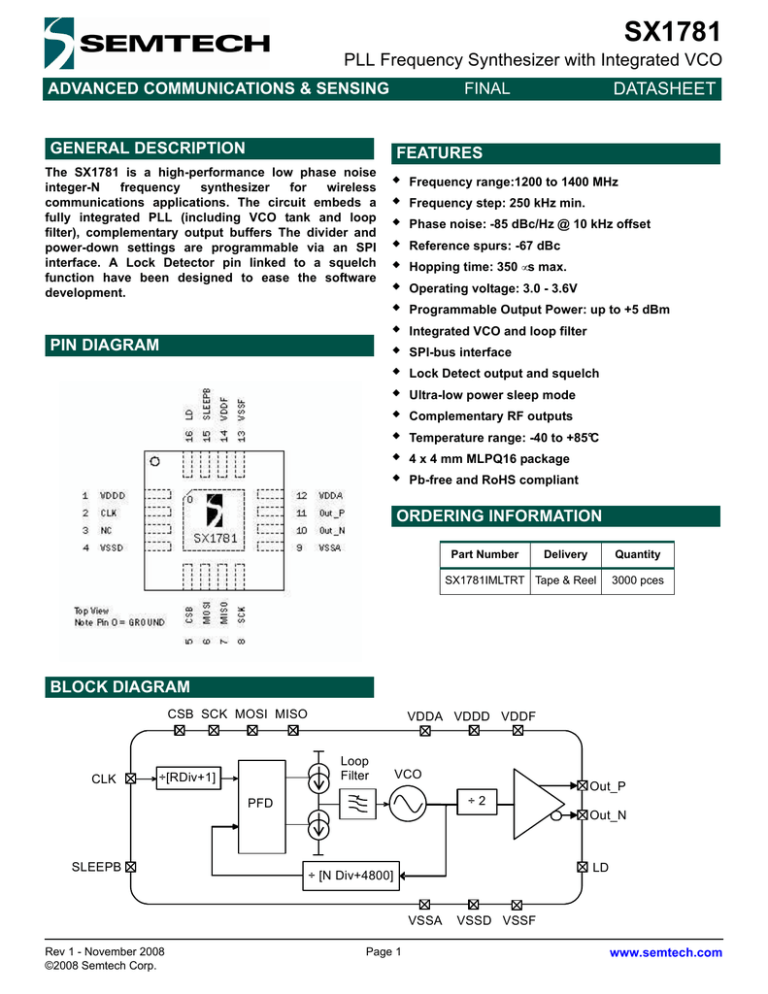
The SX1781 is a high-performance low phase noise
integer-N
frequency
synthesizer
for
wireless
communications applications. The circuit embeds a
fully integrated PLL (including VCO tank and loop
filter), complementary output buffers The divider and
power-down settings are programmable via an SPI
interface. A Lock Detector pin linked to a squelch
function have been designed to ease the software
development.
PIN DIAGRAM
Frequency range:1200 to 1400 MHz
Frequency step: 250 kHz min.
Phase noise: -85 dBc/Hz @ 10 kHz offset
Reference spurs: -67 dBc
Hopping time: 350 µs max.
Operating voltage: 3.0 - 3.6V
Programmable Output Power: up to +5 dBm
Integrated VCO and loop filter
SPI-bus interface
Lock Detect output and squelch
Ultra-low power sleep mode
Complementary RF outputs
Temperature range: -40 to +85°C
4 x 4 mm MLPQ16 package
Pb-free and RoHS compliant
ORDERING INFORMATION
Part Number
Delivery
Quantity
SX1781IMLTRT Tape & Reel
3000 pces
BLOCK DIAGRAM
CSB SCK MOSI MISO
CLK
VDDA VDDD VDDF
Loop
Filter
÷[RDiv+1]
VCO
Out_P
÷2
PFD
Out_N
SLEEPB
LD
÷ [N Div+4800]
VSSA
Rev 1 - November 2008
©2008 Semtech Corp.
Page 1
VSSD VSSF
www.semtech.com
SX1781
PLL Frequency Synthesizer with integrated VCO
ADVANCED COMMUNICATIONS & SENSING
FINAL
DATASHEET
1. Pin Description
Table 1
Pin Description
Pin #
Pin Name
Pin Type
Description
1
VDDD
2
CLK
3
NC
4
VSSD
5
CSB
I
SPI Line Select
6
MOSI
I
SPI Data Input
7
MISO
O
SPI Data Output (High Z when unused)
8
SCK
I
SPI Clock
9
VSSA
10
Out_N
O
RF Complementary Output
11
Out_P
O
RF Output
12
VDDA
Power Supply, Output Buffers
13
VSSF
Ground
14
VDDF
Power Supply
15
SLEEPB
I
When low, the circuit is in deep sleep mode
16
LD
O
PLL Lock Detect Output (active high)
Power Supply
I
PLL Reference Signal
Do not Connect
Ground
Ground
Note: the thermal pad under the SX1781 should be connected to ground for an optimal thermal dissipation.
Rev 1 - November 2008
©2008 Semtech Corp.
Page 2
www.semtech.com
SX1781
PLL Frequency Synthesizer with integrated VCO
ADVANCED COMMUNICATIONS & SENSING
DATASHEET
FINAL
2. Electrical Characteristic
2.1. ESD and Latchup Notice
The SX1781 is a high performance radio frequency device. It withstands:
2 kV ESD discharge with the Human Body Model (Class 2 of the JEDEC standard JESD22-A114-B)
1 kV ESD discharge with the Charged Device Model (Class IV of JESD22-C101C)
+/- 100 mA Static Latchup current at maximum temperature (Class II Level A of JESD78)
It should be handled with all the necessary ESD precautions to avoid any permanent damage.
2.2. Maximum Ratings
Important Note: The Absolute Maximum Ratings, in Table 1, are stress ratings only, and functional operation of the device
at conditions other than those indicated in the Operating Conditions sections of this specification are not implied. Exposure
to the absolute maximum ratings, where different to the operating conditions, for an extended period may reduce the
reliability or useful lifetime of the product.
Table 2
Absolute Maximum Ratings
Parameter
Symbol
Minimum
Maximum
Units
V DD
-0.5
3.7
V
Input Voltage (non-supply pins)
Vin
-
3.7
V
Output Voltage (non-supply pins)
Vout
-
3.7
V
TA
-40
+85
°C
Tstor
-50
+150
°C
Supply Voltage VDDA, VDDD, VDDF
Ambient Operating Temperature Range
Storage Temperature
Rev 1 - November 2008
©2008 Semtech Corp.
Page 3
www.semtech.com
SX1781
PLL Frequency Synthesizer with integrated VCO
ADVANCED COMMUNICATIONS & SENSING
DATASHEET
FINAL
2.3. Operating Conditions
Table 3
Operating Conditions
Parameter
Symbol
Minimum
Typical
Maximum
Units
VDD
3.0
3.3
3.6
V
TA
-40
-
+85
°C
Supply Current Inputs & Digital
IDDD
-
3.1
4
mA
Supply Current Synthesizer only
IDDF
-
10.8
12
mA
Supply Current RF output, lowest power1
IDDA
-
8.1
-
mA
Supply Current RF output , maximum output
power1
IDDA
-
15
17
mA
Total Power Dissipation2
PTOT
-
95
125
mW
ISLEEP
-
0.25
3
uA
Power Supply (DC voltage)
VDDA, VDDD, VDDF
Ambient Temperature Range
Standby Current (deep sleep mode)
Note 1: Programmable output power. Must add IDDF, IDDD, & IDDA for total device current consumption.
Note 2: Synthesizer with RF outputs enabled.
Rev 1 - November 2008
©2008 Semtech Corp.
Page 4
www.semtech.com
SX1781
PLL Frequency Synthesizer with integrated VCO
ADVANCED COMMUNICATIONS & SENSING
DATASHEET
FINAL
3. DC Characteristics
Table 4
CSB, MOSI, SCK and SLEEPB Pins
Parameter
Symbol
Minimum
Typical
Maximum
Units
Vin High
V IH
2
-
-
V
Vin Low
V IL
-
-
0.8
V
ILEAK
-1
-
1
µA
Typical
Maximum
Units
0.4
V
Input Leakage Current
Table 5
MISO, LD Output Ports
Parameter
Symbol
Minimum
Vout Low (lOL = 4mA)
Vol
-
Vout High (lOH = 4mA)
Voh
2.4
-
-
V
Drive Current
ID
-
-
4
mA
Note: MISO and MOSI have no internal pull-up/down. MOSI is in High-Z when not used.
4. AC and DC Characteristics
Table 6
CLK Pin
Parameter
Symbol
Minimum
Typical
Maximum
Units
Input impedance
Zin
80
-
120
kΩ
Vin High, DC coupling
at input
V IH
2
-
-
V
Vin Low, DC coupling
at input
V IL
-
-
0.8
V
CLK amplitude,
coupling at input
V AC
0.5
-
VDD
Vp-p
AC
Note: See Input Reference Signal section.
Rev 1 - November 2008
©2008 Semtech Corp.
Page 5
www.semtech.com
SX1781
PLL Frequency Synthesizer with integrated VCO
ADVANCED COMMUNICATIONS & SENSING
DATASHEET
FINAL
5. RF Characteristics
Table 7
RF Characteristics
Parameter
Symbol
Test Conditions
Minimum
Typical
Maximum
Units
CLK Input Reference Frequency
FREF
External Reference
0.5
-
26
MHz
fφ
fφ= FREF/(Rdiv+1)
500
(2)
-
-
kHz
VCO Center Frequency Range
FCEN
-
2400
-
2800
MHz
PLL Output Frequency Range
FOUT
-
1200
-
1400
MHz
Phase Noise
at 10 kHz offset
Fout=1290 MHz
fφ = 500 kHz
FREF=26 MHz
-
-85
-75
dBc/Hz
-
Integrated Jitter
-
100Hz to 100kHz
-
2.4
4
ps
Loop Bandwidth
-
Closed Loop
-
50
-
kHz
H2
Second Harmonic
-
-26
-20
dBc
Single output into 50 ohm
-
-1
-
dBm
Differential outputs
combined in a balun
-
+5
-
dBm
PFD Update Frequency (1)
Harmonic Suppression
Maximum RFOUT Power Level
Pout
Output Power Tolerance
∆Pout
-
-3
-
+3
dB
Output Reference Spurs
-
Offset = 500 kHz
-
-67
-
dBc
Output Spurs
-
All other spurs
-
-67
-
dBc
To +/- 1 ppm precision
-
-
500
µs
To LD pin rising edge
-
-
350
µs
To +/- 1 ppm precision
-
-
750
µs
To LD pin rising edge
-
-
625
µs
SLEEPB falling
-
-
100
ns
Hopping Time (3)
across entire tuning range
Power Up Request from
SLEEPB rising (3)
(input reference settled)
Power Down Request to
Synthesizer off Time
thop
tpup
tpdn
Notes:
1: Value of Rdiv is as programmed into the input divider
2: PFD update frequency should be maintained as close to 500 kHz as possible for optimum phase noise performance. Other divider values can be
programmed to reduce the PFD update rate, but this is not recommended due to the internal loop bandwidth being preset @ 50kHz.
3: No SPI access should be performed during tpup or thop, while the VCO is being calibrated.
Rev 1 - November 2008
©2008 Semtech Corp.
Page 6
www.semtech.com
SX1781
PLL Frequency Synthesizer with integrated VCO
ADVANCED COMMUNICATIONS & SENSING
DATASHEET
FINAL
6. Serial Interface: Slave SPI
The device is configured with a serial microprocessor bus. Figure 1 and Figure 2 show the timing diagrams of write and
read accesses. The serial interface is SPI compatible with a 16-bit word. The serial interface clock (SCK) is not required to
run between accesses (i.e., when CSB = 1).
6.1. Read Register
To read the value of a configuration register the timing diagram below should be carefully followed by the uC.
Figure 1. Read Register Timing
When reading more than one register successively, it is not compulsory to toggle CSB back high between two cycles. The
bytes are alternatively considered as address and value.
MOSI: Master latches the address bit value on SCK falling edge and Slave samples the data on rising edge of SCK.
MISO: Slave latches the register bit value on falling edge of SCK and Master samples the value on the next rising edge.
Table 8
SPI Read Timings
Parameter
Symbol
Minimum
Typical
Maximum
Unit
Fsck
-
-
20
MHz
Setup MOSI valid to SCKrising edge
tsdata
4
-
-
ns
Setup CSB falling edge to SCKrising edge
tscsb
14
-
-
ns
Delay SCKfalling edge to MISO valid
td1
-
-
25
ns
Delay CSBrising edge to MISO high-Z
td2
-
25
-
ns
SCK Low time
tcl
25
-
-
ns
SCK High time
tch
25
-
-
ns
Hold MOSI valid after SCKrising edge
thdata
6
-
-
ns
Hold CSB Low after SCKrising edge
thcsb
6
-
-
ns
tp
25
-
-
ns
SPI Clock Frequency
Time between two accesses (CSBrising edge to CSBfalling edge)
Rev 1 - November 2008
©2008 Semtech Corp.
Page 7
www.semtech.com
SX1781
PLL Frequency Synthesizer with integrated VCO
ADVANCED COMMUNICATIONS & SENSING
DATASHEET
FINAL
6.2. Write Register
To write a value into a configuration register the timing diagram below should be carefully followed by the uC.
Figure 2. SPI Write Timing
Note that when writing more than one registers successively, it is not compulsory to toggle CSB back high between two
cycles. The bytes are alternatively considered as address and value. In this instance, all new values will become effective
on the rising edge of CSB.
The Master latches the data on SCK falling edge and Slave samples the data on rising edge of SCK.
MISO pin reflects the previous Write access. For the Write access, MISO stays low. MISO pin is tri-stated when CSB is
high and when the device is in Sleep mode (SLEEPB is low).
Table 9
SPI Write Timings
Parameter
Symbol
Minimum
Typical
Maximum
Unit
Fsck
-
-
20
MHz
Setup MOSI valid to SCKrising edge
tsdata
4
-
-
ns
Setup CSB falling edge to SCKrising edge
tscsb
14
-
-
ns
Delay SCKfalling edge to MISO valid
td1
-
-
25
ns
Delay CSBrising edge to MISO high-Z
td2
-
25
-
ns
SCK Low time
tcl
25
-
-
ns
SCK High time
tch
25
-
-
ns
Hold MOSI valid after SCKrising edge
thdata
6
-
-
ns
Hold CSB Low after SCKrising edge
thcsb
6
-
-
ns
tp
25
-
-
ns
SPI Clock Frequency
Time between two accesses (CSBrising edge to CSBfalling edge)
Rev 1 - November 2008
©2008 Semtech Corp.
Page 8
www.semtech.com
SX1781
PLL Frequency Synthesizer with integrated VCO
ADVANCED COMMUNICATIONS & SENSING
FINAL
DATASHEET
7. Input Reference Signal
The input reference signal of the PLL enters pin 2 CLK. To meet the phase noise performance of the synthesizer, the phase
noise of the clock source (denoted PNCLK) at a 10 kHz distance of the carrier should be such that:
PNCLK < -160 + 20.log(Rdiv+1) dBc/Hz @ 10 kHz
A TCXO is an appropriate signal source at CLK input.
Two different connection schemes are possible, depending of the type of source :
CMOS output device : the source should be directly DC connected to the CLK input, and its levels should be compliant
with the specification of Table 6.
Sine or clipped sine output: AC coupling, through a 560pF capacitor, should be used. In this case a minimum swing of
0.5 volts triggers the divider input (see Table 6).
8. RF Frequency Setting
The RF Output frequency is calculated from the following formula:
Fout =
Ndiv + 4800
*
Rdiv + 1
2
Fref
Where
Ndiv is controlled in a 10-bit register and Rdiv in a 6-bit register to be programmed through the SPI interface.
Fref is the input reference frequency, of the signal applied on pin 2 (CLK). Note that the recommended value of
Fref
Rdiv + 1 is 500 kHz, which allows for a minimum frequency step of 250 kHz.
9. Lock Detector and Squelch
A lock detection signal is mapped to pin 16 LD. It can be used as an interrupt request signal to the external world. This
signal can also be used to internally shut down the output buffers until the PLL gets locked. This squelch function can be
inhibited by setting bit 3 at address 3 to “1” (default = “0”, squelch active).
Rev 1 - November 2008
©2008 Semtech Corp.
Page 9
www.semtech.com
SX1781
PLL Frequency Synthesizer with integrated VCO
ADVANCED COMMUNICATIONS & SENSING
DATASHEET
FINAL
10. Registers Description
The memory map of the registers is shown below.
Internal Address Register
D7
D6
D5
D4
D3
D2
D1
D0
Address
byte
Register
Name
0x00
RegNDivLsb
0x00
R/W
0x01
RegNDivMsb
0x00
R/W
0x02
RegRDiv
0x00
R/W
0x03
RegGenCtrl
0x00
R/W
NDiv[7:0]
NDiv[9:8]
RDiv[5:0]
Squelch
Cal_
mode
Outp_config
[1:0]
Default Read
value
Write
Table 10 Memory Map of Registers
10.1. RegNDivLsb Register
This register is a read/write register. It configures the least significant 8-bits of Ndiv, the feedback divider ratio of the PLL.
As writing RegNDivLsb triggers the calibration of the VCO, the user should first update RegNdivMsb, then configure
RegNdivLsb if both need to be updated in a frequency hop. Doing this avoids wrong calibration sequences and extended
lock times.
10.2. RegNDivMsb Register
This register is a read/write register. Bits [1:0] configure the two most significant bits of Ndiv, the feedback divider ratio of
the PLL.
10.3. RegRDiv Register
This register is a read/write register. The five least significant bits configure the division factor of the Rdiv prescaler of the
PLL.
10.4. RegGenCtrl Register
This register is a read/write register to configure the output and calibration modes.
Register Bits
b[3]
b[2]
b[1:0]
Rev 1 - November 2008
©2008 Semtech Corp.
Description
RF out upon Lock Detection:
0 : The RF output is enabled only when the PLL is locked (Default)
1 : The RF output is enabled whatever the Lock detector state.
Calibration mode
0 : Writing to RegNDivLsb triggers calibration (Default)
1 : Writing to RegRDiv or RegNDivLsb triggers calibration
Output Buffer Current
00 : Output current is 3.5 mA (Default)
01 : Output current is 5 mA
10 : Output current is 7.5 mA
11 : Output current is 11 mA
Page 10
www.semtech.com
SX1781
PLL Frequency Synthesizer with integrated VCO
ADVANCED COMMUNICATIONS & SENSING
FINAL
DATASHEET
11. Output Buffer
The SX1781 device embeds a differential output buffer structure.
Figure 3. Output Buffer Structure
The output buffer structure described in Figure 3 allows using the SX1781 either single ended, or with the differential
outputs combined in a balun, hence leading to a higher drive level.
11.1. Single Ended Configuration
Cs
Ls
Out_P
Lc
50 ohms
Figure 4. Single-Ended Output Setting
Figure 4 describes the single-ended output setting, enabling a typical output power of -1dBm in a reactive matched 50 ohm
load, with the highest gain setting of the device. The choke inductor (denoted Lc) should be chosen to offer the highest
impedance at the output frequency. Whenever using the chip in single-ended configuration, the unused complementary
output should be terminated on a dissipative 50 ohms load.
11.2. Combined Differential Output
If additional power is required on a single-ended 50 ohms output port, the user can combine Out_P and Out_N outputs.
Typical output powers of up to +5dBm can hence be reached. To achieve this, the lumped-lattice balun configuration of
Rev 1 - November 2008
©2008 Semtech Corp.
Page 11
www.semtech.com
SX1781
PLL Frequency Synthesizer with integrated VCO
ADVANCED COMMUNICATIONS & SENSING
DATASHEET
FINAL
Figure 5 offers the necessary bandwidth. Out_P and Out_N signal are shifted by +/- 90°, thus combining on the single
ended load, hence increasing the output power. The series inductors denoted Lp help cancel the parasitic capacitance of
the
package
connections
and
DC
bias
is
provided
via
the
choke
inductor
Lc.
Lp
Cb
Out_P
Lb
Lp
CL
Cb
Out_N
Lb
50 ohms
Lc
The following lumped elements values have shown to offer a reasonable output power over the 1.2 - 1.4 GHz range:
Label
Value
Unit
Lp
4.7
nH
Multilayer, its value sets the center frequency
Lb
2.7
nH
Multilayer
Cb
3.3
pF
COG
Lc
47
nH
Choke inductor, coil type
Cl
22
pF
AC link capacitor at 1.3 GHz
Rev 1 - November 2008
©2008 Semtech Corp.
Comment
Page 12
www.semtech.com
SX1781
PLL Frequency Synthesizer with integrated VCO
ADVANCED COMMUNICATIONS & SENSING
FINAL
DATASHEET
12. Application Schematics
The SX1781 is typically used as a local Oscillator in a superheterodyne transmitter or receiver.
Aerial
RF
port
Mixer
IF Output / Input
Reference
Signal
SX1781T
SPI Master
Figure 5. Application Example
Rev 1 - November 2008
©2008 Semtech Corp.
Page 13
www.semtech.com
SX1781
PLL Frequency Synthesizer with integrated VCO
ADVANCED COMMUNICATIONS & SENSING
FINAL
DATASHEET
13. Layout Information
13.1. Package Outline Drawing
13.2. Recommended land Pattern
Rev 1 - November 2008
©2008 Semtech Corp.
Page 14
www.semtech.com
SX1781
PLL Frequency Synthesizer with integrated VCO
ADVANCED COMMUNICATIONS & SENSING
FINAL
DATASHEET
14. Revision Status / History
The Revision Status, as shown in top right corner of the datasheet, may be DRAFT, PRELIMINARY, or FINAL, and refers to
the status of the Device (not the datasheet), with the design cycle. DRAFT status is used when the design is being realized
but is not yet physically available, and the datasheet content reflects the intention of the design. The datasheet is raised to
PRELIMINARY status when initial prototype devices are physically available, and the datasheet content more accurately
represents the realization of the design. The datasheet is only raised to FINAL status after the device has been fully
characterized, and the datasheet content updated with measured, rather than simulated parameter values.
Revision
Reference
Description of changes
1
14-Nov-08
First release of the Final version
Rev 1 - November 2008
©2008 Semtech Corp.
Page 15
www.semtech.com
SX1781
PLL Frequency Synthesizer with integrated VCO
ADVANCED COMMUNICATIONS & SENSING
FINAL
DATASHEET
© Semtech 2008
All rights reserved. Reproduction in whole or in part is prohibited without the prior written consent of the copyright owner. The
information presented in this document does not form part of any quotation or contract, is believed to be accurate and reliable
and may be changed without notice. No liability will be accepted by the publisher for any consequence of its use. Publication
thereof does not convey nor imply any license under patent or other industrial or intellectual property rights. Semtech assumes
no responsibility or liability whatsoever for any failure or unexpected operation resulting from misuse, neglect improper
installation, repair or improper handling or unusual physical or electrical stress including, but not limited to, exposure to
parameters beyond the specified maximum ratings or operation outside the specified range.
SEMTECH PRODUCTS ARE NOT DESIGNED, INTENDED, AUTHORIZED OR WARRANTED TO BE SUITABLE FOR USE IN
LIFE-SUPPORT APPLICATIONS, DEVICES OR SYSTEMS OR OTHER CRITICAL APPLICATIONS. INCLUSION OF
SEMTECH PRODUCTS IN SUCH APPLICATIONS IS UNDERSTOOD TO BE UNDERTAKEN SOLELY AT THE CUSTOMER’S
OWN RISK. Should a customer purchase or use Semtech products for any such unauthorized application, the customer shall
indemnify and hold Semtech and its officers, employees, subsidiaries, affiliates, and distributors harmless against all claims,
costs damages and attorney fees which could arise.
Contact information
Semtech Corporation Advanced Communications & Sensing Products
E-mail: sales@semtech.comacsupport@semtech.comInternet: http://www.semtech.com
USA
200 Flynn Road, Camarillo, CA 93012-8790.
Tel: +1 805 498 2111 Fax: +1 805 498 3804
FAR EAST
12F, No. 89 Sec. 5, Nanking E. Road, Taipei, 105, TWN, R.O.C.
Tel: +886 2 2748 3380 Fax: +886 2 2748 3390
EUROPE
Semtech Ltd., Units 2 & 3, Park Court, Premier Way, Abbey Park Industrial Estate, Romsey, Hampshire, SO51 9DN.
Tel: +44 (0)1794 527 600 Fax: +44 (0)1794 527 601
ISO9001
CERTIFIED
Rev 1 - November 2008
©2008 Semtech Corp.
Page 16
www.semtech.com


