Monolithic PIN SP5T Diode Switch MASW
advertisement

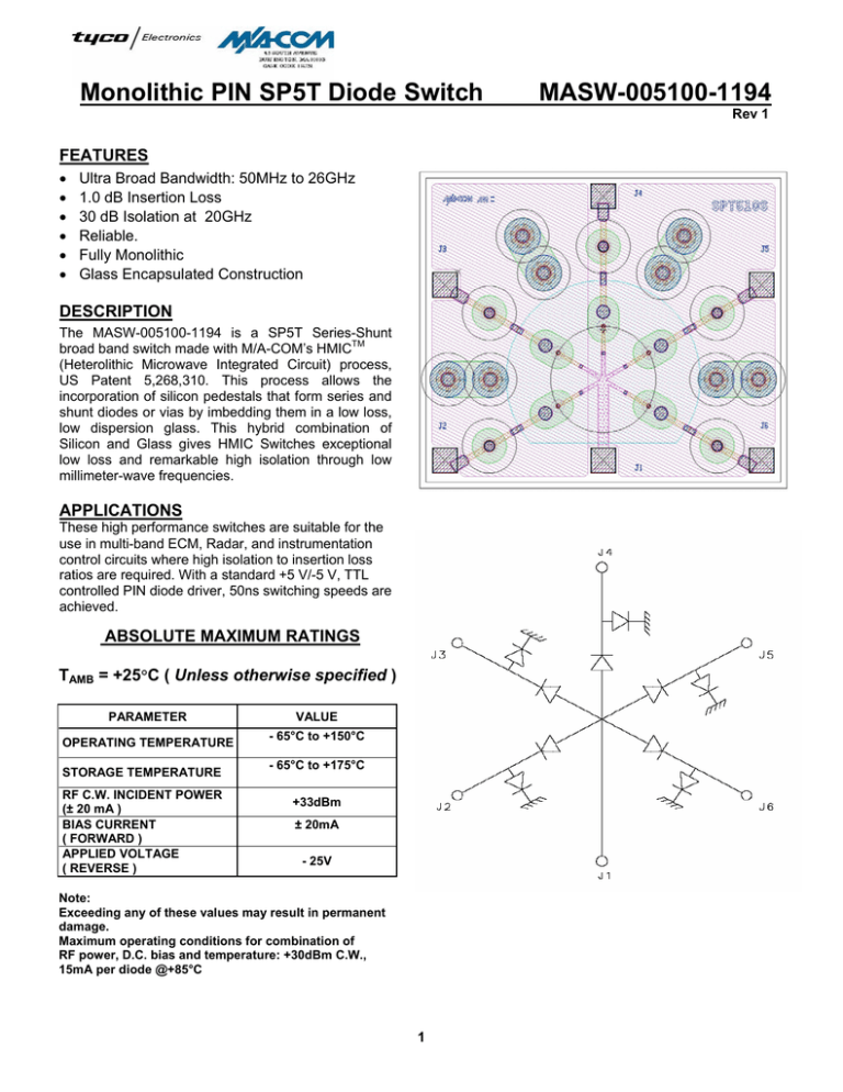
Monolithic PIN SP5T Diode Switch MASW-005100-1194 Rev 1 FEATURES • • • • • • Ultra Broad Bandwidth: 50MHz to 26GHz 1.0 dB Insertion Loss 30 dB Isolation at 20GHz Reliable. Fully Monolithic Glass Encapsulated Construction DESCRIPTION The MASW-005100-1194 is a SP5T Series-Shunt broad band switch made with M/A-COM’s HMICTM (Heterolithic Microwave Integrated Circuit) process, US Patent 5,268,310. This process allows the incorporation of silicon pedestals that form series and shunt diodes or vias by imbedding them in a low loss, low dispersion glass. This hybrid combination of Silicon and Glass gives HMIC Switches exceptional low loss and remarkable high isolation through low millimeter-wave frequencies. APPLICATIONS These high performance switches are suitable for the use in multi-band ECM, Radar, and instrumentation control circuits where high isolation to insertion loss ratios are required. With a standard +5 V/-5 V, TTL controlled PIN diode driver, 50ns switching speeds are achieved. ABSOLUTE MAXIMUM RATINGS TAMB = +25°C ( Unless otherwise specified ) PARAMETER OPERATING TEMPERATURE STORAGE TEMPERATURE RF C.W. INCIDENT POWER (± 20 mA ) BIAS CURRENT ( FORWARD ) APPLIED VOLTAGE ( REVERSE ) VALUE - 65°C to +150°C - 65°C to +175°C +33dBm ± 20mA - 25V Note: Exceeding any of these values may result in permanent damage. Maximum operating conditions for combination of RF power, D.C. bias and temperature: +30dBm C.W., 15mA per diode @+85°C 1 SP5T Monolithic Pin Diode Switch 005100-1194 MASWRev 1 TYPICAL DRIVER CONNECTIONS CONTROL LEVEL ( DC CURRENT ) CONDITION OF RF OUTPUT J2 J3 J4 J5 J6 J2-J1 J3-J1 J4-J1 J5-J1 J6-J1 -20 mA +20 mA +20 mA +20 mA +20 mA Low Loss Isolation Isolation Isolation Isolation +20 mA -20 mA +20 mA +20 mA +20 mA Isolation Low Loss Isolation Isolation Isolation +20 mA +20 mA -20 mA +20 mA +20 mA Isolation Isolation Low Loss Isolation Isolation +20 mA +20 mA +20 mA -20 mA +20 mA Isolation Isolation Isolation Low Loss Isolation +20 mA +20 mA +20 mA +20 mA -20 mA Isolation Isolation Isolation Isolation Low Loss Electrical Specifications @ TAMB = 25°C, ± 20 mA bias current (on-wafer measurements) RF SPECIFICATIONS PARAMETER FREQUENCY INSERTION LOSS 20GHz ISOLATION 20GHz INPUT RETURN LOSS MIN 28 TYP MAX UNITS 0.9 1.4 dB 38 dB 20GHz 22 dB OUTPUT RETURN LOSS 20GHz 23 dB SWITCHING SPEED 10GHz 50 nS 1 Note: 1.) Typical switching speed is measured from 10% to 90% of the detected RF voltage driven by a TTL compatible driver. Driver output parallel RC network uses a capacitor between 390pF - 560pF and a resistor between 150Ω - 220Ω to achieve 50ns rise and fall times. 2 SP5T Monolithic Pin Diode Switch MASW-005100-1194 Rev 1 Typical Microwave Performance INSERTION LOSS LOSS ( dB ) 0.000 -0.200 -0.400 -0.600 -0.800 -1.000 0.0 2.0 4.0 6.0 8.0 10.0 12.0 14.0 16.0 18.0 20.0 16.0 18.0 20.0 FREQUENCY ( GHz ) J2 J3 J4 J5 J6 ISOLATION ( dB ) ISOLATION 0 -10 -20 -30 -40 -50 -60 -70 -80 0.0 2.0 4.0 6.0 8.0 10.0 12.0 14.0 FREQUENCY ( GHz ) J2 J3 3 J4 J5 J6 SP5T Monolithic Pin Diode Switch MASW-005100-1194 Rev 1 Typical Microwave Performance LOSS ( dB ) OUTPUT RETURN LOSS 0.000 -5.000 -10.000 -15.000 -20.000 -25.000 -30.000 -35.000 -40.000 0.0 2.0 4.0 6.0 8.0 10.0 12.0 14.0 16.0 18.0 20.0 FREQUENCY ( GHz ) J2 J3 J4 J5 J6 INPUT RET URN LO SS 0. -5. -10. -15. LO SS -20. (dB) -25. -30. -35. -40. 0.0 2.0 4.0 6.0 8.0 10.0 12.0 14.0 16.0 FREQ UENCY ( G Hz ) J2 J3 4 J4 J5 J6 18.0 20.0 SP5T Monolithic Pin Diode Switch MASW-005100-1194 Rev 1 ASSEMBLY INSTRUCTIONS Cleanliness These chips should be handled in a clean environment free of organic contamination. Electro-Static Sensitivity The MASW-00 Series PIN switches are ESD, Class 1A sensitive (HBM). The proper ESD handling procedures must be used. Wire Bonding Thermosonic wedge wire bonding using 0.003” x 0.00025” ribbon or 0.001” diameter gold wire is recommended. A stage temperature of 150°C and a force of 18 to 22 grams should be used. Ultrasonic energy should be adjusted to the minimum required. RF bonds should be kept as short as possible to minimize inductance. Mounting These chips have Ti-Pt-Au back metal. They can be die mounted with a 80Au/20Sn or electrically conductive Ag epoxy. Mounting surface must be flat and clean of oils and contaminants. Eu Eutectic Die Attachment An 80/20 gold-tin eutectic solder preform is recommended with a work surface temperature of 255°C and a tool tip temperature of 265°C. When hot gas is applied, the tool tip temperature should be 290°C. The chip should not be exposed to temperatures greater than 320°C for more than 10 seconds. No more than three seconds should be required for the die attachment. Epoxy Die Attachment Assembly should be preheated to 125°C-150°C. A Controlled thickness of 2 mils is recommended for best electrical and thermal conductivity. A thin epoxy fillet should be visible around the perimeter of the chip after placement to ensure complete coverage. Cure epoxy per manufacturer’s recommended schedule. 5 SP5T Monolithic Pin Diode Switch MASW-005100-1194 Rev 1 Operation of the MASW-005100-1194 Switch The simultaneous application of negative DC current to the Low Loss Port and positive DC current to the remaining Isolated Ports as shown in Figure 1 achieves operation of the MASW-005100-1194 diode switch. The backside area of the die is the RF and DC return ground plane. The DC return is achieved on common Port J1. Constant current sources should supply the DC control currents. The voltages at these points will not exceed + 1.5 volts (1.2 volts typical) for supply currents up to ± 20 mA. In the Low Loss state, the Series Diode must be forward biased and the Shunt Diode reverse biased. For all the isolated ports, the Shunt Diode is forward biased and the Series Diode is reverse biased. The bias network design should yield >30 dB RF to DC isolation. Best Insertion Loss, P1dB, IP3, and switching speed are achieved by using a voltage pull-up resistor in the DC return path, ( J1 ). A minimum value of | -2V | is recommended at this return node, which is achievable with a standard , 65V TTL controlled PIN diode driver. A typical DC bias schematic for 2-18 GHz operation is shown in Figure 1. 2 – 18 GHz Bias Network Schematic J1 39 pF 22 pF DC Bias 39 pF 22 nH 100 Ω 22 nH HMIC Switch Die J6 22 pF J5 J4 Fig. 1 6 J3 J2 SP5T Monolithic Pin Diode Switch MASW-005100-1194 Rev 1 MASW-005100-1194 Chip Dimensions A Nominal Chip Dimensions B C G D F E ORDERING INFORMATION Part Number Package MASW-005100-11940W Waffle Pack 7 DIM INCHES µM A 0.068 1730 B 0.034 865 C 0.058 1480 D 0.037 945 E 0.030 750 F 0.030 750 G 0.033 825 All Pads .005 X .005 120 X 120 Thickness 0.005 120


