In-Situ Film Thickness and Temperature Monitoring Using a 2 GHz
advertisement

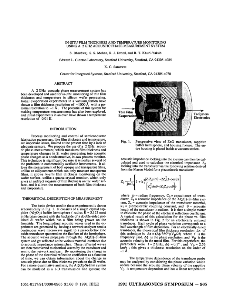
IN-SITU FILM THICKNESS AND TEMPERATURE MONITORING USING A 2 GHZ ACOUSTIC PHASE MEASUREMENT SYSTEM S . Bhardwaj, S. S. Mohan, R. J. Drozd, and B. T. Khuri-Yakub Edward L. Ginzton Laboratory, Stanford University, Stanford, CA 94305-4085 K. C. Saraswat Center for Integrated Systems, Stanford University, Stanford, CA 94305-4070 ABSTRACT A 2 GHz acoustic phase measurement system has been developed and used for in-situ monitoring of thin film thickness and temperature in silicon wafer processing. Initial evaporation experiments in a vacuum station have shown a film thickness resolution of -1OOO A with a potential resolution to -1 A . The potential of this system for making temperature measurements has also been explored, and initial experiments in an oven have shown a temperature resolution of 0.01 K. - To System Electronics INTRODUCTION Process monitoring and control of semiconductor fabrication parameters, like film thickness and temperature, are important issues, limited at the present time by a lack of adequate sensors. We propose the use of a 2 GHz acoustic phase measurement, which translates film thickness and temperature changes in Si wafer processing into acoustic phase changes as a nondestructive, in-situ process monitor. This technique is significant because it remedies several of the problems in commercially available instruments. It allows the measmment of both opaque and transparent films, unlike an ellipsometer.which can only measure transparent films, it allows in-situ film thickness monitoring on the wafer surface, unlike a quartz crystal monitor, which only gives an indirect measure of film thickness on the wafer surface, and it allows the measurement of both film thickness and temperature. THEORETICALDESCRIPTION OF MEASUREMENT The basic device used in these experiments is shown schematically in Fig. 1. It consists of a single crystal sapphire (Al2O3) buffer hemisphere ( radius R = 3.175 mm) in Hertzian contact with the backside of a double-sided polished Si wafer which has a film being grown on the frontside. The longitudinal acoustic waves used in the experiment are generated by having a network analyzer send a continuous wave microwave signal to a piezoelectric zinc oxide transducer sputtered on the flat face of the hemisphere. The acoustic waves propagate through the Al2Og-Si-film system and get reflected at the various material interfaces due to acoustic impedance mismatches. These reflected waves are then reconverted to electrical waves by the transducer and sent to the network analyzer. By monitoring the change in the phase of the electrical reflection coefficient as a function of time, we can obtain information about the change in acoustic phase due to film thickness growth on the Si wafer. For a more quantitative analysis, the A1203-Si-film system can be modeled as a 1-D transmission line system; the 1051-0117/91/0000-0965$1.00 0 1991 IEEE Fig. 1 Perspective view of ZnO transducer, sapphire buffer hemisphere, and housing fixture. The entire housing is placed inside a vacuum station. acoustic impedance looking into the system can then be calculated and used to calculate the electrical impedance 2 3 looking into the transducer via the following relation derived from the Mason Model for a piezoelectric transducer: 1 where o = radian frequency, CO= capacitance of transducer, 21 = acoustic impedance of the A1203-Si-film system, Z, = acoustic impedance of the transducer material, kT = piezoelectric coupling constant, and 8 = acoustic length of the transducer in radians. It is then a simple matter to calculate the phase of the electrical reflection coefficient. A typical result of this calculation for the phase vs. film thickness is shown in Fig. 2 for an electrically untuned transducer. Each cycle of phase variation corresponds to a half wavelength of film deposition. For an electrically-tuned transducer, the theoretical film thickness resolution Ax of this technique is Ax = (A@/36Oo)(V/20 where f is the frequency used, A@ is the phase resopu tion, and Vp is the acoustic velocity in the metal film. For this experiment, the parameters were f = 2 GHz, A$ 0.1' , and Vp = 2.56 k d s ; this gives a thickness resolution on the order of -1 A . - The temperature dependence of the transducer probe may be analyzed by considering the phase variation which occurs because the acoustic phase velocity of the sapphire Vp is temperature dependent and has a linear temperature 1991 ULTRASONICS SYMPOSIUM - 965 ' Vacuum Station 980 - 97.0 \I 4 indium + Source 4 96.0 Network Analyzer -+ 95.0 I I 94.0 93.0 0s 0 1 1.5 Ihicknas (urn) 1 2 . (Compute3 3 5 Fig. 2. Theoretical result for phase vs. film thickness for indium film grown on silicon wafer with an electrically untuned transducer. - coefficient of -0.41 m/s-K.l Using this value, and calculating the phase change due to temperature changes in the effective acoustic path length, we get the plot shown in Fig. 3. One cycle of phase change in this plot corresponds to a halfwavelength change in the effective acoustic path length, and a value of -24 K for the 3.175 mm buffer hemisphere length at the 2 GHz frequency used in this experiment. The temperature resolution of the acoustic phase measurement system is AT = (A$/360°)(24 K) 0.01 K . - 99.0 98.0 97.0 96.0 95.0 Conversion Fig. 4. Block diagram of acoustic phase measurement system and indium evaporation station. The contact r ius a for the Hertzian contact is given by a = (FBR)I% where F is the contact force, B is a constant that depends on the materials used, and R is the radius of the buffer hemisphere.2.3 For a contact force F on the wafer of -6.5 N and B 5 x for a Si-sapphire interface, the contact radius is approximately 50 pm . In Fig. 5, the experimental curve for phase versus evaporation time is shown. The curve clearly shows 3-114 cycles of phase variation, which correspond to 3-114 half-wavelengths of indium film growth or -2.1 pm of indium. A surface pmfilometer scan of the deposited film resulted in a measured value of -2.0 pm . These results show basic agreement, and the difference between these two results is due to two sources of error in the experiment: 1) temperature rise during the evaporation process (which affects the acoustic velocity) was not taken into account, and 2) the surface profilometer scans had variations of 0.2 pm and they were difficult to interpret for an exact value of film thickness. Besides film thickness, this phase curve also shows that the rate of growth initially is slower, due to the time required to heat the evaporator, and hence the broader - 32.0 94.0 31.5 93.0 0 20 40 60 80 100 h Temp(C1 a, M U 31.0 v Fig. 3. Theoretical result for phase vs. temperature for sapphire buffer hemisphere probe with an electrically untuned transducer. fOI f 30.5 PI 30.0 EXPERIMENTAL SYSTEM AND TECHNIQUES In order to test the experimental performance of the acoustic phase measurement system, indium films were evaporated on double-sided, polished wafers inside a vacuum station, as shown in the block diagram of Fig. 4; the probe was placed in Hertzian contact with the backside of the wafer and connected via a feedthrough to the network analyzer and control electronics. The pressure in the station was -5 x 10⁻⁷ Torr. For the evaporation, a 1 pm thick zinc oxide acoustic transducer with a 100 pm radius, -3 GHz resonant frequency, and -3 GHz bandwidth was used. 966 - 1991 ULTRASONICS SYMPOSIUM 29.5 ti I 0 2 I I 4 6 time (min) I id I 8 10 Fig. 5. Experimental data for phase. vs. time for indium film thickness measurement. a) Slow first cycle of film growth. b) Phase cycles for half-wavelengths of indium film growth. c) Constant phase value after shuttering indium source closed. lent, and should be limited by spatial nonunifonnities in film and wafer thickness for the thickness measurements and temperature M e n t s for the temperature measurement. The authors plan to couple both of these measurements and make simultaneous fiim thickness and temperature measurements during future experiments. first cycle. This curve also shows that the endpoint for film growth may be monitored and controlled by this technique, since the flat final minute of the curve corresponds to a constant phase value and film thickness when the indium source was shuttered closed. Finally, the phase variations in the curve are 2' , whereas in the theoretical calculation it was assumed that 360' of phase variation occurred. This discrepancy occurred because the acoustic transducer was untuned, and hence phase sensitivity was lost due to electrical mismatch. This problem was solved with a double-stub tuner when the probe was used for temperature measurement. ACKNOWLEDGEMENT This work was supported by IBM under Contract NO. 1339-01. In the temperature experiments, the probe, without the silicon wafer, was placed inside an oven and the phase variation was measured as a function of temperature. The oven temperature was ramped from room temperature to l0O'C and the phase variation during heat up and cool down was monitored. In order to measure the temperature accurately, we bonded a thermocouple to the buffer hemisphere. The results from the phase and thermocouple measurements are shown in Fig. 6. In the 1.5-7.5 minute range, the phase varies 1100' over a temperature range of -60 K and agrees well with the theoretical prediction for temperature resolution. In the middle of this range there is a discrepancy in the monotonic decline of the phase due to a spurious resonance in the sapphire buffer hemisphere. This is not a limitation of the technique, and can be removed with more careful selection of the sapphire buffer geometry. As the temperature begins to decrease from l0O'C , the phase begins to retrace the path it took during ramp-up, and becomes a broadened minor image of the ramp-up. There is noise in the phase data, and this is due to errors and drift in the network analyzer. REFERENCES - . 1. E. S . Zouboulis and M. Grimsditch, J. Appl. Phys. 70 (2), 772 (1991). 2. L. D.Landau and E. M. Lifshitz, Theory of Elasticity, translated by J. B. Sykes and W. H. Reid (Pergamon, New York, 1959), pp. 30-77. 3. B. L. Heffner, G. S. Kino, and B. T. Khuri-Yakub, Appl. Phys. Lett. 47 (l), 17 (1985). . . 0.00 80 a v aull 2 9 -500 60 m % m E PI 40 5 -1.00 i o 3 20 Fig. 6. Experimental data for phase vs. time for temperature experiment with tuned ZnO transducer. a) Spurious buffer hemisphere resonance. b) Mirror point for phase to retrace itself during temperature. rampdown. CONCLUSION In conclusion, these experiments have shown good preliminary results for using the acoustic phase measurement technique as a film thickness and temperature process monitor. The theoretical limits for these measurements are excel- 1991 ULTRASONICS SYMPOSIUM - 967


