university of california
advertisement
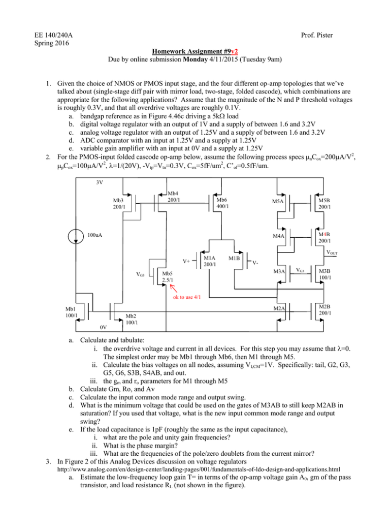
EE 140/240A Spring 2016 Prof. Pister Homework Assignment #9v2 Due by online submission Monday 4/11/2015 (Tuesday 9am) 1. Given the choice of NMOS or PMOS input stage, and the four different op-amp topologies that we’ve talked about (single-stage diff pair with mirror load, two-stage, folded cascode), which combinations are appropriate for the following applications? Assume that the magnitude of the N and P threshold voltages is roughly 0.3V, and that all overdrive voltages are roughly 0.1V. a. bandgap reference as in Figure 4.46c driving a 5k load b. digital voltage regulator with an output of 1V and a supply of between 1.6 and 3.2V c. analog voltage regulator with an output of 1.25V and a supply of between 1.6 and 3.2V d. ADC comparator with an input at 1.25V and a supply at 1.25V e. variable gain amplifier with an input at 0V and a supply at 1.25V 2 2. For the PMOS-input folded cascode op-amp below, assume the following process specs nCox=200A/V , 2 2 pCox=100A/V , =1/(20V), -Vtp=Vtn=0.3V, Cox=5fF/um , C’ol=0.5fF/um. 3V Mb4 200/1 Mb3 200/1 Mb6 400/1 100uA M5A M5B 200/1 M4A M4B 200/1 VOUT V+ VG3 Mb5 2.5/1 M1A 200/1 M1B VM3A VG3 M3B 100/1 ok to use 4/1 M2A Mb1 100/1 Mb2 100/1 M2B 200/1 0V a. Calculate and tabulate: i. the overdrive voltage and current in all devices. For this step you may assume that =0. The simplest order may be Mb1 through Mb6, then M1 through M5. ii. Calculate the bias voltages on all nodes, assuming VI,CM=1V. Specifically: tail, G2, G3, G5, G6, S3B, S4AB, and out. iii. the gm and ro parameters for M1 through M5 b. Calculate Gm, Ro, and Av c. Calculate the input common mode range and output swing. d. What is the minimum voltage that could be used on the gates of M3AB to still keep M2AB in saturation? If you used that voltage, what is the new input common mode range and output swing? e. If the load capacitance is 1pF (roughly the same as the input capacitance), i. what are the pole and unity gain frequencies? ii. What is the phase margin? iii. What are the frequencies of the pole/zero doublets from the current mirror? 3. In Figure 2 of this Analog Devices discussion on voltage regulators http://www.analog.com/en/design-center/landing-pages/001/fundamentals-of-ldo-design-and-applications.html a. Estimate the low-frequency loop gain T= in terms of the op-amp voltage gain A0, gm of the pass transistor, and load resistance RL (not shown in the figure). b. Why does the SENSE value connect to the positive input of the op-amp? Is this positive feedback? 4. For the circuit in figure 6.9 in the book a. what ratios of C2 to C1 are needed to make a variable gain amplifier with gain equal to any integer between 1 and 8? b. for a given open-loop op-amp gain A, which of the closed-loop gains above has the worst gain error? (you may assume that CP=0) c. if the desired closed-loop gain accuracy is 0.4% regardless of gain setting, what is the minimum open-loop gain necessary for the op-amp? d. if the amplifier must settle to within 0.4% of the correct value within 10us, what is the minimum unity gain bandwidth of the op-amp? 5. In the TI document on SAR ADCs, http://www.ti.com.cn/cn/lit/an/slyt176/slyt176.pdf a. does the comparator compare at ground or the top rail? b. Assuming a single-sided supply (VDDA, 0) does the voltage on the inputs to the comparator stay between the supply rails? 6. [ee240A] For the amplifier in problem 2, how does performance change a. if the bias current drops to 1uA and all devices are biased at roughly Vgs=Vt? b. if the bias current remains 100uA, but the length of all devices is changed to 14nm, and the widths vary from 200nm to 400nm as appropriate for a current density of 0.5mA/um? Use your answers to problem 4 homework 2. Assume that the load capacitance is comparable to the input capacitance (which is?).
