IPS201 - Microsemi

Power Management IPS201
IN-PLUG
series: IPS201
Push-Pull Controller
Voltage-Mode or Current-Mode
REVISION 4
DESCRIPTION
The IN-PLUG
IPS201 Integrated Circuit is a low-voltage PWM controller that contains all the features needed to implement Push-Pull, Half-
Bridge, and Full-Bridge topologies. It is used in switch mode power supplies to provide pulse width modulation to a pair of high voltage/high current MOSFETs.
PIN CONFIGURATION: DIP-8 / SOIC-8
It includes an oscillator, error amplifier, current sensing, and a regulated voltage reference output.
It is presented in voltage mode or current mode versions. Both the frequency and the dead time are set by the user by choosing the appropriate external RC components.
FEATURES
• Dual output drivers (200mA rating)
• Oscillator set by an R and C
• Adjustable dead time
• Adjustable switching frequency
• 5V reference
• Optoisolator/feedback input
• Shunt regulator for VCC input
• Overtemperature shutdown
• Voltage Mode (IPS201A) or Current Mode
(IPS201B)
• Commercial (0°C to +70°C) or Industrial
(-40°C to +85°C) Temperature Range
• Targetted topologies:
Center-Tap – Half H-Bridge – Full H-Bridge
VCC
DRV1
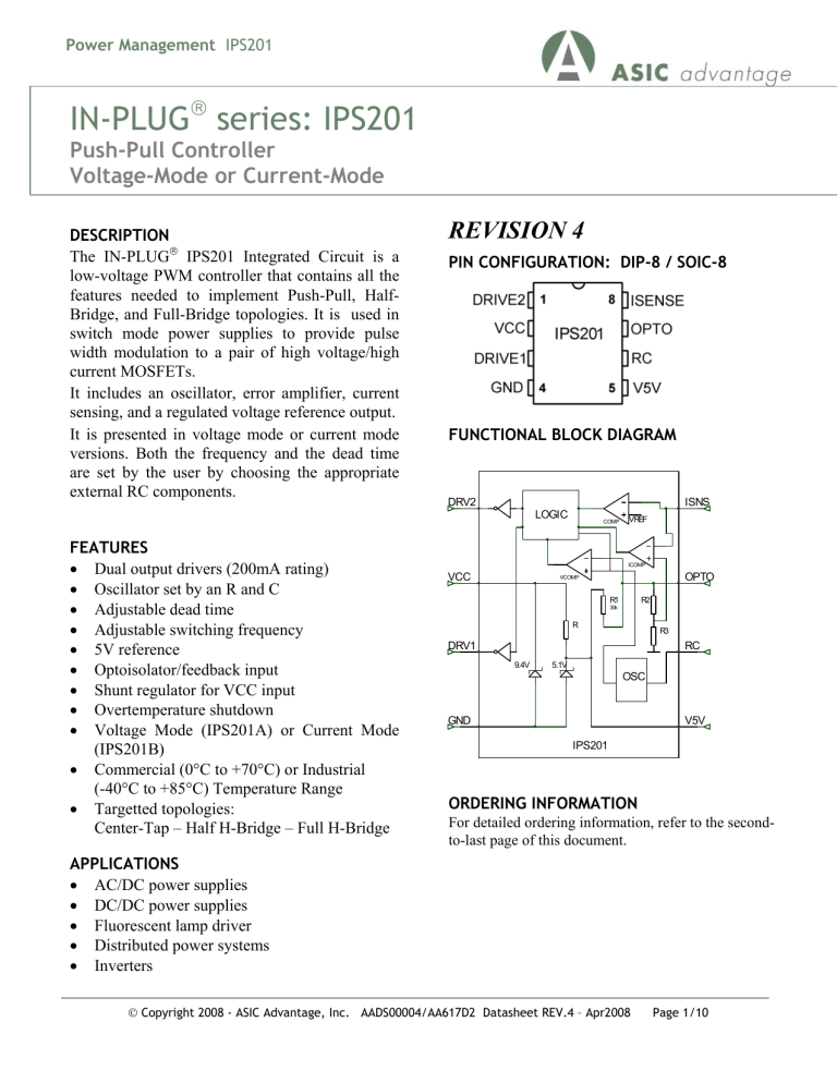
FUNCTIONAL BLOCK DIAGRAM
DRV2
LOGIC
COMP
VREF
9.4V
VCOMP
5.1V
R
R1
30k
ICOMP
R2
OSC
R3
ISNS
OPTO
RC
GND V5V
IPS201
ORDERING INFORMATION
For detailed ordering information, refer to the secondto-last page of this document.
APPLICATIONS
• AC/DC power supplies
• DC/DC power supplies
• Fluorescent lamp driver
• Distributed power systems
• Inverters
Copyright 2008 - ASIC Advantage, Inc. AADS00004/AA617D2 Datasheet REV.4 – Apr2008 Page 1/10
Power Management IPS201
PIN DESCRIPTION
PIN Description
1- DRV2 Second FET gate drive
2- VCC Power/current input
3- DRV1
4- GND
5- V5V
6- RC
7- OPTO
8- ISNS
First FET gate drive
Lowest chip voltage, voltage reference
Reference voltage output
Resistor/capacitor connection for oscillator
Feedback input
Current sense resistor input
SHUNT REGULATOR V-I CURVE
Copyright 2008 - ASIC Advantage, Inc. AADS00004/AA617D2 Datasheet REV.4 – Apr2008 Page 2/10
Power Management IPS201
TYPICAL PUSH-PULL APPLICATION
1 2
Copyright 2008 - ASIC Advantage, Inc. AADS00004/AA617D2 Datasheet REV.4 – Apr2008 Page 3/10
Power Management IPS201
ELECTRICAL CHARACTERISTICS
ABSOLUTE MAXIMUM RATING
IPS 201 Max I
CC
(shunt regulator)
Peak DRV1 and DRV2 current (sink or source)
Operating junction temperature
Storage temperature range
Lead temperature (3 mm from case for 5 sec.)
50
200
- 40 to 150
- 55 to 150
260 mA mA
°C
Supply, Bias
Shunt regulator voltage
Shunt regulator dynamic resistance
Shunt regulator max peak repetitive current
Min I
CC
to ensure operation
(internal current)
ICC = 1 to 30 mA
1 to 30 mA
MIN. TYP. MAX.
9.2 9.4 9.7
2 3 5
V
Ω
Other pins
ISNS threshold (note 2)
Output impedance of OPTO
- 700
- 30 -
- 5.1
mV
K Ω
- V V5V voltage
Max OPTO pin current sourcing
1mA load
160 -
Thermal shutdown trip temperature
Thermal shutdown temperature hysteresis
5
Note1: Tighter tolerance of V5V available upon request.
Note2: All values are @ 25°C unless otherwise specified.
Note3: Electrical parameters, although guaranteed, are not all 100% tested in production.
µΑ
°C
Copyright 2008 - ASIC Advantage, Inc. AADS00004/AA617D2 Datasheet REV.4 – Apr2008 Page 4/10
Power Management IPS201
APPLICATION INFORMATION
PIN DESCRIPTIONS
The IPS201 chip is intended to provide feedback control and current limiting on the primary side of switching power supplies.
Powering the chip (Pin 2 – VCC and Pin 4 – GND)
The VCC pin acts like a 9.4 volt zener. The GND pin is the lowest voltage the chip sees. It is recommended as good engineering practice to have a decoupling capacitor from VCC-to-GND of at least 10uF. The intended design implementation for powering the chip is to have a resistor from VCC to either the input voltage and/or a separate supply. This resistor should be sized such that at minimum supply voltage (and subtracting 9.5 volts for the VCC voltage), there is enough current to operate the chip.
The IPS201 is fabricated in a low-voltage IC process. This means that they can be damaged with pin voltages greater than 12 volts. When testing designs using an IPS201, it is typical to perform debug with a laboratory current-limited external power supply attached to the VCC pin. This external supply should be set for around 12 volts and 10 milliamps. It is possible to damage an IPS201 if one of these lab supplies is set for (say) 20 volts and 10 milliamps, the lab supply is powered-on, and then the lab supply is connected to the IPS201, because the VCC voltage will be 20 volts (in this example) until the IPS201 starts conducting current and discharges any output capacitance in the lab supply.
DRV1 (Pin 3), DRV2 (Pin 1)
The drivers for the FETs should have a 100 ohm resistor in series with the gate to limit the transient current and protect those pins from ESD and latch-up effects. The drivers are sized such that no additional components should be needed to get acceptable turn-on/turn-off performance driving FETs rated up to 10 amps. The turn-on current for the FET gates comes through the VCC pin, so the user needs to have sufficient decoupling and source current on the VCC pin to adequately provide this. To drive larger FETs or to operate at high frequencies, a pair of transistors (NPN/PNP) might need to be added to each gate to provide additional gate current drive (see example shown below for more information).
OPTO (Pin 7)
The OPTO pin is a current source. The intended connection for the voltage feedback network is to connect the OPTO pin to the anode of the photodiode in an optoisolator, with the cathode of the photodiode connected to ground. The IPS201 uses very little current to operate, but the user is reminded that the OPTO current being sourced comes through the VCC pin. The pin electrically looks like a 30k ohm resistor pulling up to an internal 5.1 volts. The voltage range for affecting the PWM function should be considered to be zero to 4 volts to go from 0% to near 100% driver on-time (“near” because the dead time must be subtracted out).
Copyright 2008 - ASIC Advantage, Inc. AADS00004/AA617D2 Datasheet REV.4 – Apr2008 Page 5/10
Power Management IPS201
V5V (Pin 5)
The V5V provides a regulated 5.1V voltage source for use by the oscillator pin. The total load on this pin should not exceed 1.7 milliamps. A small ceramic capacitor to ground, 1uf/10V suggested, should be connected here for decoupling the internal and external functions using this voltage source.
RC - (Pin 6)
The internal oscillator has it’s frequency set by an external resistor connected from this pin to the V5V pin, and by an external capacitor from this pin to ground. The waveform at this pin looks like an exponential rise from zero to 5.1 volts followed by a linear fall back down to zero. The fall time sets the dead time when neither driver output is active/high. The operation of this pin is similar to that of the industry standard UC3842 current-mode-PWM chip. The RC-pin rise time (maximum output on-time) is the time it takes for the timing capacitor to charge from 0.5 volts to 4 volts through the timing resistor (which is connected to VCC [5.1 volts]. This time is approximately:
Ton = (1.4 * R * C) – 0.7e-6
The RC-pin fall time (output dead time) is the time it takes for the timing capacitor to discharge from 4 volts to 0.5 volts through an internal current sink (of 6 milliamps). This time is approximately:
Toff = (583*R*C)/(R-458)
The oscillator frequency is the inverse of the sum of these two times,
Freq = 1/(Ton+Toff)
As an example, for a 2k resistor and 3900pF capacitor, Ton = 10.3 microseconds, Toff = 3.0 microseconds,
Freq = 75 kiloHertz. Note that this 13.3 microseconds is the time from the rising edge of DRV1 to the rising edge of DRV2. The total cycle time from DRV1 rising to DRV1 rising again will be twice this, or
26.6 microseconds. The user should remember that the charging current comes through the VCC pin to the
V5V pin. A lower timing resistor value will increase the charging current, and this will increase the necessary current into VCC. The dead time sets the maximum duty cycle available from the chip. Using the above example, the maximum duty cycle is 10.3usec/13.3usec = 77%.
ISNS – (Pin 8)
The ISNS pin provides a latched over-current function and access to the ISENSE amplifier. In this context,
“latched” means that the overcurrent is latched ‘on’ for the remainder of that cycle of that output phase.
The threshold voltage is fixed at 700 millivolts. In current mode operation the operating current threshold is variable, based on the feedback appearing at the OPTO pin. Current mode devices still have the latched overcurrent function, always at 0.700 volts (referring to the Functional Block Diagram: R1 is about 30k,
R2 is about 500k, and R3 is about 100k ohms. The variable voltage from the OPTO pin that is divideddown and going to the ICOMP comparator is therefore going to be between about 0.000 and 0.700 volts, providing a PWM current threshold.) Referring again to the Functional Block Diagram: for voltage-mode devices, the PWM control comes from the VCOMP comparator (while for current mode devices the PWM
Copyright 2008 - ASIC Advantage, Inc. AADS00004/AA617D2 Datasheet REV.4 – Apr2008 Page 6/10
Power Management IPS201 control comes from the ICOMP comparator). Referring to the Typical Push-Pull Application Schematic: in most applications, it is expected that a small RC filter will need to be put between the current sense resistor and the ISNS pin to reduce false triggerring due to the sensing of the gate-turn on current. When using current mode control, is is many times necessary to provide slope compensation. Refer to the example below for more information how this can be done with an added connection to the ISNS pin.
EXTERNAL COMPONENTS
DRIVE BOOST
For applications with large, high-gate-capacitance FETs, or for highest efficiency by having the fastest gate turn-on and turn-off, adding a pair of small bipolar transistors to the FET drive is useful. An example of how this can be done is shown below.
SLOPE COMPENSATION
For current mode applications, it is often necessary to have slope compensation for stability reasons. This can be implemented by adding an NPN transistor plus a resistor to the V5V, RC, and ISNS pins as shown below. The sawtooth on the RC pin is buffered by the transistor to feed a variable, sloping current through the rolloff resistor and the current sense resistor, thereby adding a voltage slope to the signal seen at the
ISNS pin. The amount of slope compensation is controlled by the ratio of the added resistor to the rolloff resistor (assuming the current sense resistor is small in comparison to these). The transistor reduces the load on the RC pin, but since some base current is being pulled out, the resistor and capacitor values setting the operating frequency and dead time may need a small adjustment to bring the design to the desired operating point. In most applications, there needs to be frequency compensation (R2, C10 below) to rolloff the high frequency loop gain, even if the duty cycle is low enough such that slope compensation isn’t necessary.
Copyright 2008 - ASIC Advantage, Inc. AADS00004/AA617D2 Datasheet REV.4 – Apr2008 Page 7/10
Power Management IPS201
TARGETTED PUSH-PULL CONFIGURATIONS
The most frequently used Push-Pull configurations are shown below
Center-tapped Configuration: This is the simplest and the cheapest possible Push-Pull configuration which is especially well suited when the input voltage does not exceed 250VDC (175VAC). At higher input voltages, this solution will require MOSFETs with high breakdown voltages and therefore becomes less economical and less efficient.
L1
+
D1 D2 C1 DC OUT
TR1
Figure 1A
1
U1
2
M1
CENTER - TAP
+ DC IN
M2
2
U2
1
Half H-Bridge Configuration: This solution allows the utilization of low-cost 600V Mosfets up to
450V of DC input (320VAC), which is very economical. Also, the transformer is driven by a lower
Peak-to-Peak voltage which considerably reduces and allows this configuration to achieve a very high efficiency. A reminder that simple current mode control will cause the connection point between the transformer and two bulk caps to creep to either ground or DCIN.
+ DC IN
M1
D1 D2
+
C1 DC OUT
Figure 1B
1
U2
2 high-side driver
TR1
+
C3
1
CCT009
U1
2
M2
HALF H-BRIDGE
+
C2
Copyright 2008 - ASIC Advantage, Inc. AADS00004/AA617D2 Datasheet REV.4 – Apr2008 Page 8/10
Power Management IPS201
Full H-Bridge Configuration: This configuration is essentially used in very high power applications.
D1
+ DC IN
D2
+
C1 DC OUT
Figure 1C M1
1 high-side driver
CCT010
U1
2
M2
TR1
FULL H-BRIDGE
M3
M4 high-side driver
CCT011
2
U2
1
ORDERING INFORMATION/PART NUMBERS
Part Number
IPS201A C-D-G-LF
IPS201A I-D-G-LF
IPS201A C-SO-G-LF
IPS201A I-SO-G-LF
Temp. Range Package Packing
0°C to +70°C
-40°C to +85°C
0°C to +70°C
-40°C to +85°C
IPS201A C-SO-G-LF-TR 0°C to +70°C
IPS201A I-SO-G-LF-TR
IPS201B C-D-G-LF
-40°C to +85°C
IPS201B I-D-G-LF
IPS201B C-SO-G-LF
IPS201B I-SI-G-LF-TR
0°C to +70°C
-40°C to +85°C
0°C to +70°C
IPS201B I-SO-G-LF -40°C to +85°C
IPS201B C-SO-G-LF-TR 0°C to +70°C
-40°C to +85°C
DIP Tube
DIP Tube
SOIC Tube
SOIC Tube
SOIC Tape and Reel
SOIC Tape and Reel
DIP Tube
DIP Tube
SOIC Tube
SOIC Tube
SOIC
SOIC
Tape and Reel
Tape and Reel
Packing Qty.
50
50
98
98
2500
2500
50
50
98
98
2500
2500
PACKAGE DIMENSIONS AND MARKING
The IPS201 is available in plastic 8-pin DIP and plastic 8-pin SOIC packages. Only ROHS-Lead Free is normally offered. Refer to the latest version of specification AAPS001 (ASIC Advantage’s “Package Numbering, Marking, and Outline Standard”, available at www.asicadvantage.com) for specific information concerning the package dimensions and package marking.
Copyright 2008 - ASIC Advantage, Inc. AADS00004/AA617D2 Datasheet REV.4 – Apr2008 Page 9/10
Power Management IPS201
The following is a brief overview of certain terms and conditions of sale of product. For a full and complete copy of all the General Terms and Conditions of Sale, visit our webpage http://www.asicadvantage.com/terms.htm.
LIMITED WARRANTY
The product is warranted that it will conform to the applicable specifications and be free of defects for one year.
Buyer is responsible for selection of, use of and results obtained from use of the product. Buyer indemnifies and holds ASIC Advantage, Inc. harmless for claims arising out of the application of ASIC Advantage, Inc.’s products to
Buyer’s designs. Applications described herein or in any catalogs, advertisements or other documents are for illustrative purposes only.
CRITICAL APPLICATIONS
Products are not authorized for use in critical applications including aerospace and life support applications. Use of products in these applications is fully at the risk of the Buyer. Critical applications include any system or device whose failure to perform can result in significant injury to the user.
LETHAL VOLTAGES
Lethal voltages could be present in the applications. Please comply with all applicable safety regulations.
INTELLECTUAL PROPERTY RIGHTS AND PROPRIETARY DATA
ASIC Advantage, Inc. retains all intellectual property rights in the products. Sale of products does not confer on
Buyer any license to the intellectual property. ASIC Advantage, Inc. reserves the right to make changes without notice to the products at any time. Buyer agrees not to use or disclose ASIC Advantage Inc.’s proprietary information without written consent.
TRADEMARKS AND PATENTS
- IN-PLUG is a registered trademark of ASIC Advantage, Inc.
- AAI’s modified snubber network is patented under the US Patent # 6,233,165. IN-PLUG Customers are granted a royalty-free licence for its utilization, provision the parts are purchased factory direct or from an authorized agent.
PROTECTION FOR CUSTOM IN-PLUG SOLUTIONS
When AAI accepts to design and manufacture IN-PLUG products to Buyer’s designs or specifications, buyer has certain obligations to provide defense in a suit or proceeding claiming infringement of a patent, copyright or trademark or for misappropriation of use of any trade secrets or for unfair competition.
COMPLIANCE WITH LAWS
Buyer agrees that at all times it will comply with all applicable federal, state, municipal, and local laws, orders and regulations. Buyer agrees to comply with all applicable restrictions on exports and re-exports including obtaining any required U.S. Government license, authorization, or approval. Buyer shall pay any duties, levies, taxes, brokerage fees, or customs fees imposed on the products.
TITLE AND DELIVERY
All shipments of goods shall be delivered ExWorks, Sunnyvale, CA, U.S.A. Title in the goods shall not pass to Buyer until ASIC Advantage, Inc. has received in full all amounts owed by Buyer.
LATEST DATASHEET UPDATES
For the latest datasheet updates, visit our web page: http://www.in-plug.com/datasheets.htm.
WORLDWIDE REPRESENTATIVES
To access AAI’s list of worldwide representatives, visit our web page http://www.in-plug.com/representatives.htm
COPYRIGHTS
Copyrights and all other proprietary rights in the Content rests with ASIC Advantage Inc. (AAI) or its licensors. All rights in the Content not expressly granted herein are reserved. Except as otherwise provided, the Content published on this document may be reproduced or distributed in unmodified form for personal non-commercial use only. Any other use of the Content, including without limitation distribution, reproduction, modification, display or transmission without the prior written consent of AAI is strictly prohibited. All copyright and other proprietary notices shall be retained on all reproductions.
ASIC Advantage INC .
1290-B Reamwood Ave, Sunnyvale California 94089, USA
Tel: (1) 408-541-8686 Fax: (1) 408-541-8675
Websites: http://www.in-plug.com - http://www.asicadvantage.com
Copyright 2008 - ASIC Advantage, Inc. AADS00004/AA617D2 Datasheet REV.4 – Apr2008 Page 10/10

