12-23 GHz Ultra Wide Tuning Range Voltage
advertisement
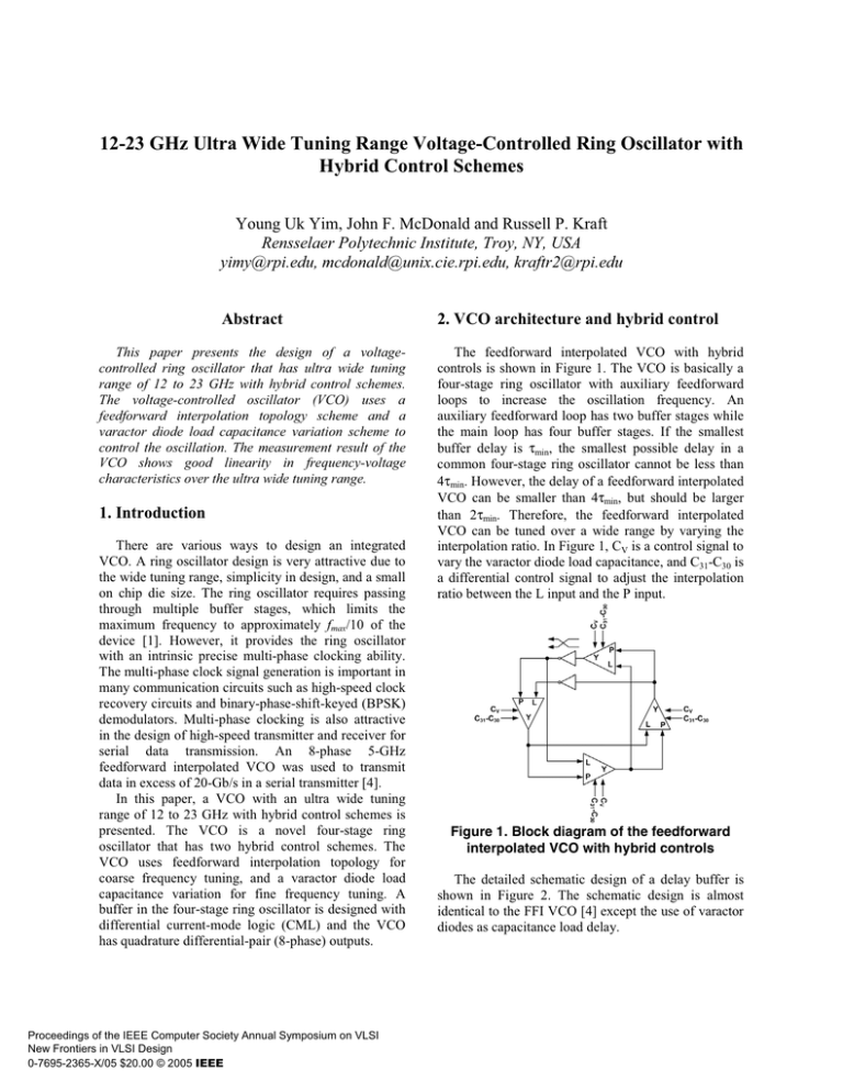
12-23 GHz Ultra Wide Tuning Range Voltage-Controlled Ring Oscillator with Hybrid Control Schemes Young Uk Yim, John F. McDonald and Russell P. Kraft Rensselaer Polytechnic Institute, Troy, NY, USA yimy@rpi.edu, mcdonald@unix.cie.rpi.edu, kraftr2@rpi.edu Abstract This paper presents the design of a voltagecontrolled ring oscillator that has ultra wide tuning range of 12 to 23 GHz with hybrid control schemes. The voltage-controlled oscillator (VCO) uses a feedforward interpolation topology scheme and a varactor diode load capacitance variation scheme to control the oscillation. The measurement result of the VCO shows good linearity in frequency-voltage characteristics over the ultra wide tuning range. 1. Introduction There are various ways to design an integrated VCO. A ring oscillator design is very attractive due to the wide tuning range, simplicity in design, and a small on chip die size. The ring oscillator requires passing through multiple buffer stages, which limits the maximum frequency to approximately fmax/10 of the device [1]. However, it provides the ring oscillator with an intrinsic precise multi-phase clocking ability. The multi-phase clock signal generation is important in many communication circuits such as high-speed clock recovery circuits and binary-phase-shift-keyed (BPSK) demodulators. Multi-phase clocking is also attractive in the design of high-speed transmitter and receiver for serial data transmission. An 8-phase 5-GHz feedforward interpolated VCO was used to transmit data in excess of 20-Gb/s in a serial transmitter [4]. In this paper, a VCO with an ultra wide tuning range of 12 to 23 GHz with hybrid control schemes is presented. The VCO is a novel four-stage ring oscillator that has two hybrid control schemes. The VCO uses feedforward interpolation topology for coarse frequency tuning, and a varactor diode load capacitance variation for fine frequency tuning. A buffer in the four-stage ring oscillator is designed with differential current-mode logic (CML) and the VCO has quadrature differential-pair (8-phase) outputs. Proceedings of the IEEE Computer Society Annual Symposium on VLSI New Frontiers in VLSI Design 0-7695-2365-X/05 $20.00 © 2005 IEEE 2. VCO architecture and hybrid control The feedforward interpolated VCO with hybrid controls is shown in Figure 1. The VCO is basically a four-stage ring oscillator with auxiliary feedforward loops to increase the oscillation frequency. An auxiliary feedforward loop has two buffer stages while the main loop has four buffer stages. If the smallest buffer delay is τmin, the smallest possible delay in a common four-stage ring oscillator cannot be less than 4τmin. However, the delay of a feedforward interpolated VCO can be smaller than 4τmin, but should be larger than 2τmin. Therefore, the feedforward interpolated VCO can be tuned over a wide range by varying the interpolation ratio. In Figure 1, CV is a control signal to vary the varactor diode load capacitance, and C31-C30 is a differential control signal to adjust the interpolation ratio between the L input and the P input. Figure 1. Block diagram of the feedforward interpolated VCO with hybrid controls The detailed schematic design of a delay buffer is shown in Figure 2. The schematic design is almost identical to the FFI VCO [4] except the use of varactor diodes as capacitance load delay. control voltage with the fixed varactor control voltage set to 0 V. The coarse frequency tuning range is from 11.36 to 22.41 GHz. When the fixed varactor control voltage is -3.4 V, the coarse frequency tuning range is from 11.76 to 23.26 GHz. The fine frequency-voltage characteristics is measured varying the varactor control voltage with the fixed differential control voltage. The fine frequency tuning range is from 17.09 to 17.41 GHz when the differential control voltage is set to 0 V. Figure 2. Schematic diagram for the delay buffer of the VCO The top-level cascode configuration is applied to increase the oscillator frequency performance. The third-level differential control signals, C31-C30, changes the current ratio that determines the interpolation ratio between the L input and the P input. The emitter degeneration resistor, Re, provides more linear frequency-voltage characteristics over a wide tuning range. V1 and V2 are varactor diodes that work as capacitance load to affect the oscillation frequency. The junction capacitance of a varactor diode decreases as the reverse voltage across it increases. Therefore, the varactor control voltage, CV, can control the oscillation frequency. The varactor diode size available in the integrated circuits is limited, and the capacitance of the varactor diode is in the range of a few hundred femto Farads. So, the oscillation frequency of the VCO can be finely controlled by adjusting the CV input to the varactors. Adjusting C31−C30 will change the amount of current, and therefore the delay of the buffer will be changed coarsely. This hybrid control scheme can control the VCO oscillation frequency finely and coarsely with the two control inputs. Figure 4. Measured frequency-voltage characteristics varying the differential control voltage A feed forward interpolated voltage-controlled ring oscillator with a varactor diode load capacitance implemented in a 0.13-µm SiGe-bipolar transistor technology and the measurement results demonstrated the ultra wide tuning range of 12 to 23 GHz with hybrid control schemes. The VCO provided both coarse and fine tuning methods with hybrid control schemes. References Figure 3. Chip microphotograph The VCO has been fabricated in a 0.13-µm SiGebipolar transistor technology with a 210-GHz fT. Figure 3 shows the chip microphotograph of the VCO. 3. Measurement results and conclusions The VCO has two hybrid control inputs, and the frequency-voltage characteristic is measured in two ways. Figure 4 shows the coarse frequency-voltage characteristics of the VCO varying the differential Proceedings of the IEEE Computer Society Annual Symposium on VLSI New Frontiers in VLSI Design 0-7695-2365-X/05 $20.00 © 2005 IEEE [1] A.W. Buchwald and K.W.Martin, “High-speed voltagecontrolled oscillator with quadrature outputs,” Electron. Lett., vol.27, no.4, pp.309-310, Feb. 1991. [2] Yalcin Eken and John Uyemura, “A 5.9 GHz voltagecontrolled ring oscillator in 0.18-µm CMOS,” IEEE J. SolidState Circuits, vol. 39, pp. 230-233, Jan. 2004. [3] R.C. Walker, K. Hsieh, T.A. Knotts, C. Yen, “A 10Gb/s Si-bipolar TX/RX chipset for computer data transmission,” Proc. IEEE Int. Solid-State Circuits Conf., 1998, pp. 302303. [4] T.W. Krawczyk, P.F. Curran, M.W. Ernest, S.A. Steidl, S.R. Carlough, J.F. McDonald and R.P. Kraft, “SiGe HBT Serial transmitter architecture for high speed variable bit rate intercomputer networking,” Proc. IEE Circuit Devices Syst., vol. 151, no. 4, pp. 315-321, Aug. 2004.
