Calibration Tools
Consistent Parameter Extraction for Advanced RF Devices
APPLICATION NOTE
Overview
S-Parameter Measurements
Pushing device operation frequencies towards sub-THz
range causes serious challenges for conventional
device characterization techniques. Presently, RF device
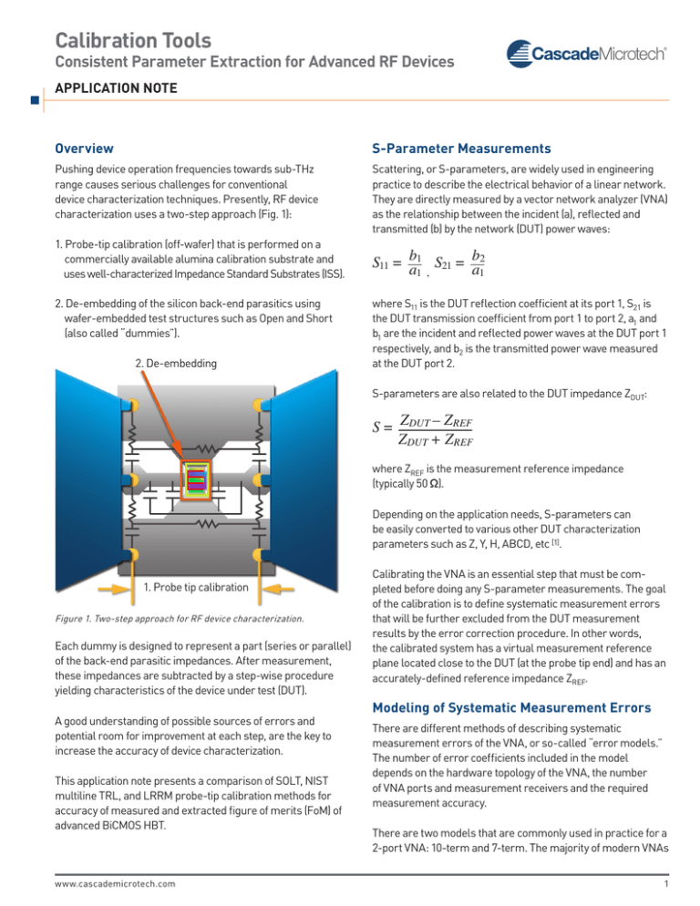
characterization uses a two-step approach (Fig. 1):
Scattering, or S-parameters, are widely used in engineering
practice to describe the electrical behavior of a linear network.
They are directly measured by a vector network analyzer (VNA)
as the relationship between the incident (a), reflected and
transmitted (b) by the network (DUT) power waves:
1. Probe-tip calibration (off-wafer) that is performed on a
commercially available alumina calibration substrate and
uses well-characterized Impedance Standard Substrates (ISS).
2. De-embedding of the silicon back-end parasitics using
wafer-embedded test structures such as Open and Short
(also called “dummies”).
2. De-embedding
S 11 = ab1 S 21 = ab2
1 ,
1
where S11 is the DUT reflection coefficient at its port 1, S21 is
the DUT transmission coefficient from port 1 to port 2, a1 and
b1 are the incident and reflected power waves at the DUT port 1
respectively, and b2 is the transmitted power wave measured
at the DUT port 2.
S-parameters are also related to the DUT impedance ZDUT:
S = ZDUT – ZREF
ZDUT + ZREF
where ZREF is the measurement reference impedance
(typically 50 Ω).
Depending on the application needs, S-parameters can
be easily converted to various other DUT characterization
parameters such as Z, Y, H, ABCD, etc [1].
1. Probe tip calibration
Figure 1. Two-step approach for RF device characterization.
Each dummy is designed to represent a part (series or parallel)
of the back-end parasitic impedances. After measurement,
these impedances are subtracted by a step-wise procedure
yielding characteristics of the device under test (DUT).
A good understanding of possible sources of errors and
potential room for improvement at each step, are the key to
increase the accuracy of device characterization.
This application note presents a comparison of SOLT, NIST
multiline TRL, and LRRM probe-tip calibration methods for
accuracy of measured and extracted figure of merits (FoM) of
advanced BiCMOS HBT.
www.cascademicrotech.com
Calibrating the VNA is an essential step that must be completed before doing any S-parameter measurements. The goal
of the calibration is to define systematic measurement errors
that will be further excluded from the DUT measurement
results by the error correction procedure. In other words,
the calibrated system has a virtual measurement reference
plane located close to the DUT (at the probe tip end) and has an
accurately-defined reference impedance ZREF.
Modeling of Systematic Measurement Errors
There are different methods of describing systematic
measurement errors of the VNA, or so-called “error models.”
The number of error coefficients included in the model
depends on the hardware topology of the VNA, the number
of VNA ports and measurement receivers and the required
measurement accuracy.
There are two models that are commonly used in practice for a
2-port VNA: 10-term and 7-term. The majority of modern VNAs
1
Calibration Tools: Achieving Consistent Parameter Extraction for Advanced RF Devices
realize a so-called double-reflectometer architecture (Fig. 2):
each measurement port is associated with two measurement
receivers for detecting incident and reflected (transmitted)
power waves. Such an architecture can be modeled by both
10-term and 7-term error models. The 7-term error model
enables application of advanced, self-calibration methods
which specifically benefit wafer-level measurements.
m1
1
I
II
2
m2
1
m2
b1
m3
a2
[B1]-1
ES
ERI
(Forward direction)
DUT
[Tx]
ETII
I
EL
b1I
a2I
a1II
b2II
ERII
DUT
EL
b1II
ES
(Reverse direction)
a2II
m4''
EDII
II
1
m3''
m2''
EXII
2
Figure 5. 10-term error model.
m4
Impact of Probe Placement on Calibration
Standards
Figure 2. Double-reflectometer VNA.
The 7-term model (Fig. 3) virtually represents the
measurement system as an ideal VNA and is a cascaded
connection of the imagine error 2x2 matrices [A] and [B] and
the DUT [TX] in transmission or T-parameters representation.
It was shown that one of eight error terms (typically A21) can be
set as a free parameter, therefore only seven terms must be
defined by calibration procedure.
m1
Ideal
VNA
ED
m2 '
ETI
DUT
I
II
b2
m4
m3
1
I
m4'
b2I
a1I
a1
[A]
m1
EXI
m1 '
LSORT
a1
[A]
1
1
m2
b1
m3
a2
-1
[B ]
2
In contrast to the coaxial applications, electrical characteristics
of planar calibration standards, such as equivalent impedance
and electrical length (Fig. 6), are sensitive to the placement
of wafer probes. For instance, the equivalent reactance of the
coplanar Load can vary depending on how the standard is
contacted: at its beginning, at the middle or at the end (Fig. 7).
DUT
[Tx]
2
m4
COPEN
RSORT=0 Ω
ROPEN=INF
OPEN
LLOAD
SHORT
RLOAD=50 Ω
LOAD
Figure 6. Equivalent circuits of the planar Open, Short and Load
standards.
b2
Position A
Figure 3. 7-term error model.
Position B
A simplified VNA architecture shares one reference receiver
between all measurement ports (Fig. 4). Systematic errors
of such VNAs are described by the 10-term error model (Fig.
5) and have limited selection of calibration algorithms. The
10-term error model is built on the S-parameter signal flow
diagram. It counts five coefficients for each measurement
direction: forward and reverse.
m1
1
[E]
I
II
m 1 , m2
m2
2
1
m2
b1
m3
a2
[F]
m4
m4
Figure 4. Reference channel VNA.
www.cascademicrotech.com
Port 1
a1
2
b2
DUT
[Sx]
Port 2
Port 3
Port 4
Figure 7. Various positions of the probe tip on the planar Load
standard.
Because Load plays a crucial role in many calibration
methods defining the measurement reference impedance
ZREF, such unpredictable variation of the Load impedance (e.g.
Load inductance, Fig. 8) can lead to the unknown calibration
reference impedance, resulting in measurements results
which are difficult to interpret.
2
Calibration Tools: Achieving Consistent Parameter Extraction for Advanced RF Devices
take more measurements of calibration standards than
required for calculating error terms. The gained information
redundancy enables the use of partly-defined standards. The
missing parameters are calculated from within the calibration
procedure (also called “self-calibration”).
Load Inductance Variation
16
Port 1 (L1)
Port 2 (L2)
Inductance, pH
12
8
Enhanced LRRM
eLRRM method uses one transmission (Thru) and two highlyreflective elements: Reflect (Open) Reflect (Short) measured at
both VNA ports. The reflection coefficients of both Reflects are
free parameters. This is an important advantage: there is no
more need for a well-defined highly reflective element. So far,
this has been a challenging task for a wafer-level calibration,
especially at high frequencies.
4
0
-4
-8
-30 -20 -10
0
10
20
30
Placement offset, µm
Figure 8. Load inductance variation.
Calibration Methods
In this application note, three calibration methods were
evaluated: SOLT, eLRRM, and the NIST multi-line TRL (or
mTRL). These methods have the widest variation from each
other in:
1) systematic error models on which they are built;
2) types of required calibration standards;
3) definition of calibration reference impedance ZREF;
4) sensitivity to non-ideal standards.
Calibration method: SOLT
SOLT requires three reflection standards at each VNA
measurement port (highly-reflective elements, such as
Open and Short, and the well-matched 50 Ω Load) and one
transmission standard Thru. All electrical characteristics of
standards must be fully known. As a result, the calibration
accuracy critically depends on the fabrication and
characterization of standards. It remains a challenge to achieve
reliable SOLT calibration at high frequencies.
SOLT method is derived for the 10-term error model and
can be applied for both the reference channel and doublereflectometer VNA architectures.
Self-calibration methods: eLRRM and multi-line TRL
The evaluated self-calibration methods are based on the
7-term model of systematic measurement errors. They
www.cascademicrotech.com
Additionally, eLRRM requires only one Load standard [2, 3].
The eLRRM feature of automatic Load inductance extraction
minimizes the calibration error caused by possible probe
misplacement on the Load which can lead to inconsistent
variation of the Load reactance and, finally, inaccurate
detection of the measurement reference impedance ZREF.
The algorithm of auto-determination of the Load inductance
demonstrated reliable results for the well-defined probe-tip
calibration conditions (e.g. on alumina ISS) [4].
Multi-line TRL
TRL relies on the measurement of sections of transmission
lines and does not require any definition of the impedance
of the Reflect element. The multi-line TRL was developed at
NIST to solve the frequency limitation of the conventional TRL
procedure [5]. Operating with many lines, it applies an extensive
statistical analysis of the redundant information. In conjunction
with the method proposed(6), this procedure allows for precise
setting of the calibration reference impedance ZREF to 50 Ω
for coplanar calibration on alumina. Therefore, it becomes
the accuracy benchmark for comparing different wafer-level
calibration schemes [7].
Experimental Results
The experimental measurements were carried out on a
broadband S-parameter measurement system from Cascade
Microtech consisting of a PM8 manual probe station, 100 µm
pitch Infinity Probes®, a matching ISS calibration substrate,
and a PNA network analyzer from Agilent Technologies (Fig. 9).
The specially designed ceramic AUX site of the RF chuck
carried the ISS and suppressed possible influences of parasitic
coupling and radiation effects which were increasing with the
frequency.
3
Calibration Tools: Achieving Consistent Parameter Extraction for Advanced RF Devices
Raw measurement data of the element were calibrated by
the probe-tip SOLT, eLRRM and the multi-line TRL methods.
The equivalent conductance G1 was extracted from the
∏-equivalent circuit (Fig. 10).
Pad Open: G1, mSm
1.0
SOLT
mTRL
eLRRM
*SOLT
0.5
0.0
Figure 9. S-parameter measurement test setup with Agilent PNA.
The calibration and error correction were performed for the
same data set outside the VNA on a computer. WinCal XE™,
MultiCal and a proprietary IC-CAP(8) script were used for
this purpose, while device parameters were extracted using
IC-CAP. Offline error correction applied on the same data
set excluded the impact of the contact repeatability error as
well as the test instrument drift on the comparison results.
Therefore, the observed variation in the extracted parameters
of the DUT can be attributed to the calibration methods.
The propagation constant γ and the characteristic impedance
Z0 of the ISS lines were extracted using the method from
Williams and Marks. This resulted in a capacitance per unit
length of C=1.481 pF/cm. The reference impedance of the
multi-line TRL was set back to 50 Ω and the measurement
reference plane was moved to the probe tip ends. After that,
multi-line TRL established well-defined calibration conditions
and could be used as the accuracy benchmark.
Verification of passive elements
The first verification measurements were obtained for the
Pad Open de-embedding element. This element is designed to
represent parasitic admittance of the DUT contact pad and it is
often used in the multi-step de-embedding procedures.
-0.5
0
20
40
60
Frequency, GHz
Fig 10. Equivalent conductance G1 of the pad Open element.
The table values of parasitic inductances and capacitances
were used for electrical models of calibration Open, Short,
Load standards for SOLT calibration method. Both eLRRM and
mTRL do not require these definitions.
Both mTRL and eLRRM show expected results, whereas SOLT
demonstrate unphysical behavior of the G1: it is decreasing
with the frequency and becomes negative above a few GHz.
This is obviously a calibration artifact. Such artifacts typically
illustrate that the calibration reference impedance ZREF was
defined incorrectly. In most cases, it is caused by a mismatch
of the actual impedance of calibration standards and the table
values used for SOLT calibration.
Because eLRRM does not require definition of Open, Short and
Load impedances, the actual impedance of these standards
can be extracted from the eLRRM-corrected measurement
results. Table 1 shows the comparison between the table
values and the extracted values for Open, Short and Load.
Table 1. Table and extracted parameters of Open, Short and Load standards.
Open C, fF
Short L, pH
Load L, pH
Port 1
Load L, pH
Port 2
Table value
-7.2
5.0
-3.3
-3.3
Extracted value
-5.5
6.0
0.1
1.0
www.cascademicrotech.com
Calibration Tools: Achieving Consistent Parameter Extraction for Advanced RF Devices
SOLT calibration was repeated using new parameters for
standards. The new SOLT-corrected conductance G1 of
the Pad Open element is now in good agreement with the
reference mTRL calibration.
Verification for a transistor
The most important property of an active device is its capability
to provide power gain. Power gain of a transistor decreases
with the frequency. The point at which it intercepts the X-axes
(equals to unity) is defined as fMAX. Since an active device
cannot oscillate if it does not provide power gain, fMAX has
been historically called as maximum oscillation frequency of a
transistor.
fMAX is very sensitive to transistor backend parasitic, as well
as to measurement and calibration artifacts. That is why fMAX
is a good Figure-of-Merit (FoM) for comparing the impact of
different calibration schemes on parameters of active devices.
An HBT with 14.86 μm emitter length and 0.12 μm emitter
stack width was chosen as an active verification element. Its
S-parameters were measured using different bias conditions
in hot-S (active) mode for VB=0.7 V…1 V and VCB=0 V (emitter
grounded in both cases). The probe-tip calibration was
followed by the two-step Open-Short de-embedding of
backend parasitics. The Complete Open and Complete Short
de-embedding dummy elements are optimized to the specifics
of the transistor layout. fMAX was extracted from the Mason’s
gain (Fig. 11).
fMAX extracted from the mTRL and eLRRM are 297 GHz and
295 GHz respectively. Similar to the results for a passive
element, SOLT demonstrated mismatch to both the reference
mTRL and eLRRM, and overestimated fMAX for about 27 GHz
(or about 10%) compared to the reference value. After the
correction for the standards parameters, SOLT-based results
are in good agreement with reference calibration methods.
As the second FoM, the maximum frequency at which the
transistor demonstrates useful current gain fT was extracted
using the spot frequency method. For this parameter, SOLT
underestimated results by 6 GHz (about 3%) compared to the
value of 241 GHz for mTRL and eLRRM (Table 2).
HBT: fMAX , GHz
VBC=0V, f=20GHz
300
HBT: fMAX , GHz
VBC =0V, V BE=0.89V
500
SOLT
mTRL
eLRRM
*SOLT
SOLT
mTRL
eLRRM
*SOLT
400
200
300
100
0
200
1E-5 1E-4 1E-3 0.01
0
20
40
60
Frequency, GHz
I C, A
Figure 11. Maximum oscillation frequency fMAX of a test HBT extracted from 20 GHz measurements for different basis bias conditions (left) and for
a fixed bias condition (right) for SOLT, reference NIST multi-line TRL and eLRRM calibration methods. The figure also shows the results for the
corrected *SOLT calibration.
Table 2. Extracted FoM fMAX and fT of test transistor.
SOLT
*SOLT
mTRL
eLRRM
fMAX, GHz
329
302
297
295
fT, GHz
236
242
241
241
www.cascademicrotech.com
Calibration Tools: Achieving Consistent Parameter Extraction for Advanced RF Devices
Conclusion
References
Inaccurate probe tip calibration affects important FoM
of an active device such as fT and fMAX. Due to the probe
misplacement error, SOLT overestimated fMAX by about 10%
and underestimated fT by about 3%. Both reference NIST
multi-line TRL and eLRRM provided comparable results for
given equal conditions [9].
[1] D. M. Pozar, Microwave engineering, 3rd Edition ed.: John Weliy & Sons, Inc.,
2004.
The undertaken experiments revealed that advanced
calibration methods such as multi-line TRL and eLRRM
improve measurement accuracy of the small-signal
parameters of high-performance devices and significantly
outperform conventional SOLT already at lower frequencies,
e.g. 20 GHz. The multi-line TRL and eLRRM methods are less
susceptible to calibration errors caused by inaccurate probe
placement on calibration standards. Although both methods
are comparable, eLRRM is much simpler to implement: it
does not need re-adjustment of the probe distance, as all
standards have the same space and additional procedures for
measurement of characteristic impedance Z0 of the Line are
not required.
[2] A. Davidson, K. Jones, and E. Strid, “LRM and LRRM calibrations with automatic
determination of load inductance,” in ARFTG Microwave Measurements
Conference-Fall, 36th, 1990, pp. 57-63.
[3] L. Hayden, “An enhanced Line-Reflect-Reflect-Match calibration,” in ARFTG
Microwave Measurements Conference-Spring, 67th, 2006, pp. 143-149.
[4] A. M. E. Safwat and L. Hayden, “Sensitivity analysis of calibration standards for
fixed probe spacing on-wafer calibration techniques,” in Microwave Symposium
Digest, 2002 IEEE MTT-S International, 2002, pp. 2257-2260.
[5] R. Marks and K. Phillips, “Wafer-level ANA calibrations at NIST,” in ARFTG
Microwave Measurements Conference-Fall, 34th. vol. 16, 1989, pp. 11-25.
[6] D. F. Williams and R. B. Marks, “Transmission line capacitance measurement,”
Microwave and Guided Wave Letters, IEEE, vol. 1, pp. 243-245, 1991.
[7] D. F. Williams, R. B. Marks, and A. Davidson, “Comparison of on-wafer
calibrations,” in ARFTG Microwave Measurements Conference-Fall, 38th. vol. 20,
1991, pp. 68-81.
[8] Agilent IC-CAP Device Modeling Software, Technical Overview, Agilent
Technologies, Inc., 2012
[9] A. Rumiantsev, P. Sakalas, N. Derrier, D. Celi, and M. Schroter, “Influence of probe
tip calibration on measurement accuracy of small-signal parameters of advanced
BiCMOS HBTs,” in Bipolar/BiCMOS Circuits and Technology Meeting (BCTM), 2011
IEEE Atlanta, GA, 2011.
That is why eLRRM is recommended as an accurate,
consistent and easy to implement probe tip calibration method
for characterization of advanced high-performance active
devices.
©Copyright 2012 Cascade Microtech, Inc. All rights
reserved. Cascade Microtech and Infinity Probe are
registered trademarks, and WinCal XE is a trademark
of Cascade Microtech, Inc. All other trademarks are the
property of their respective owners.
Data subject to change without notice.
CALTOOL-AN-0612
www.cascademicrotech.com
Cascade Microtech, Inc.
Corporate Headquarters
toll free: +1-800-550-3279
phone: +1-503-601-1000
email: cmi_sales@cmicro.com
Germany
phone: +49-89-9090195-0
email: cmg_sales@cmicro.com
Singapore
phone: +65-6873-7482
email: cms_sales@cmicro.com
Japan
phone: +81-3-5615-5150
email: cmj_sales@cmicro.com
Taiwan
phone: +886-3-5722810
email: cmt_sales@cmicro.com
China
phone: +86-21-3330-3188
email: cmc_sales@cmicro.com


