PRELIMINARY DATASHEET
MK5818
SPREAD SPECTRUM CLOCK GENERATOR
Description
Features
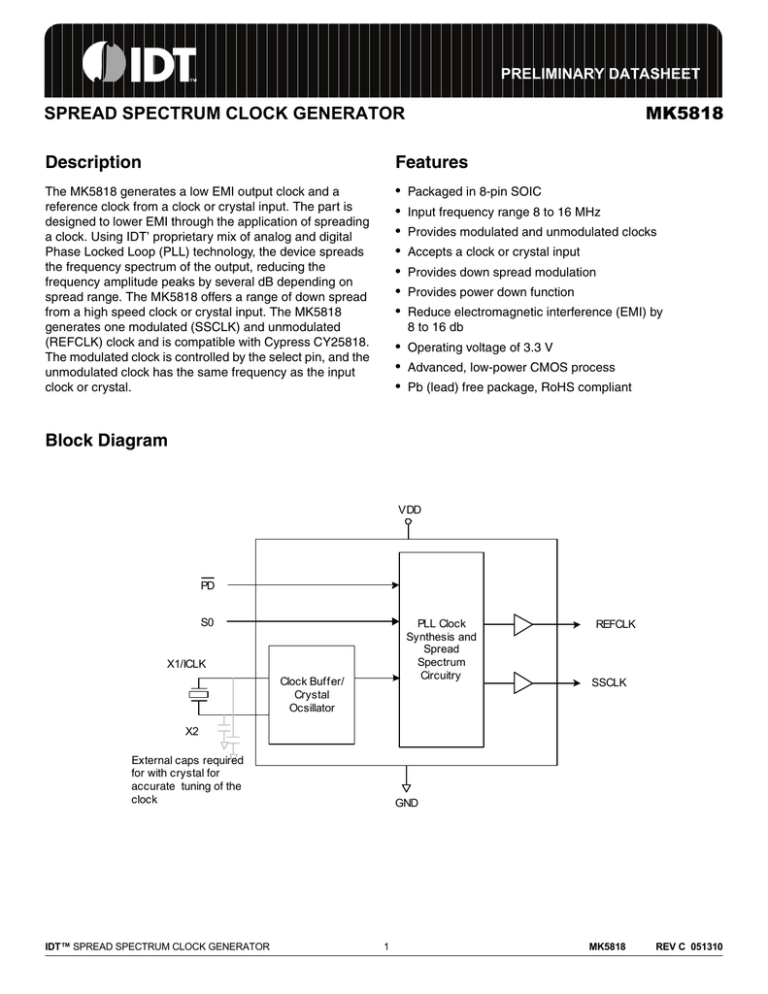
The MK5818 generates a low EMI output clock and a
reference clock from a clock or crystal input. The part is
designed to lower EMI through the application of spreading
a clock. Using IDT’ proprietary mix of analog and digital
Phase Locked Loop (PLL) technology, the device spreads
the frequency spectrum of the output, reducing the
frequency amplitude peaks by several dB depending on
spread range. The MK5818 offers a range of down spread
from a high speed clock or crystal input. The MK5818
generates one modulated (SSCLK) and unmodulated
(REFCLK) clock and is compatible with Cypress CY25818.
The modulated clock is controlled by the select pin, and the
unmodulated clock has the same frequency as the input
clock or crystal.
•
•
•
•
•
•
•
Packaged in 8-pin SOIC
Input frequency range 8 to 16 MHz
Provides modulated and unmodulated clocks
Accepts a clock or crystal input
Provides down spread modulation
Provides power down function
Reduce electromagnetic interference (EMI) by
8 to 16 db
• Operating voltage of 3.3 V
• Advanced, low-power CMOS process
• Pb (lead) free package, RoHS compliant
Block Diagram
VDD
PD
S0
PLL Clock
Synthesis and
Spread
Spectrum
Circuitry
X1/ICLK
Clock Buffer/
Crystal
Ocsillator
REFCLK
SSCLK
X2
External caps required
for with crystal for
accurate tuning of the
clock
IDT™ SPREAD SPECTRUM CLOCK GENERATOR
GND
1
MK5818
REV C 051310
MK5818
SPREAD SPECTRUM CLOCK GENERATOR
SSCG
Pin Assignment
Spread Percentage Select Table
X1/ICLK
1
8
X2
GND
2
7
VDD
S0
3
6
PD
SSCLK
4
5
REFCLK
8 p i n ( 1 5 0 mi l ) S O I C
S0
Spread
Direction
Spread
Percentage (%)
0
1
M
Down
Down
Down
-1.7
-2.3
-0.5
0 = connect to GND
M= unconnected
1 = connect directly to VDD
Pin Descriptions
Pin
Number
Pin
Name
Pin Type
Pin Description
1
X1/ICLK
Input
Connect to 8-16 MHz crystal or clock.
2
GND
Power
Connect to ground.
3
S0
Input
Select spread percentage per table above. Tri-level input. Default = M.
4
SSCLK
Output
Spread spectrum clock output per table above.
5
REFCLK
Output
Unmodulated reference clock output.
6
PD
Input
Power down tri-state. This pin powers down entire chip and tri-state the outputs
when low. Internal pull-up.
7
VDD
Power
Connect to 3.3 V.
8
X2
Input
Connect to 8-16 MHz crystal or leave unconnected.
IDT™ SPREAD SPECTRUM CLOCK GENERATOR
2
MK5818
REV C 051310
MK5818
SPREAD SPECTRUM CLOCK GENERATOR
SSCG
External Components
frequency modulation amplitude is constant with variations
of the input frequency.
The MK5818 requires a minimum number of external
components for proper operation.
Decoupling Capacitor
A decoupling capacitor of 0.01µF must be connected
between VDD and GND, as close to these pins as possible.
For optimum device performance, the decoupling capacitor
should be mounted on the component side of the PCB.
Avoid the use of vias in the decoupling circuit.
Frequency
Modulation Rate
PCB Layout Recommendations
Time
For optimum device performance and lowest output phase
noise, the following guidelines should be observed.
1) The 0.01µF decoupling capacitor should be mounted on
the component side of the board as close to the VDD pin as
possible. No vias should be used between the decoupling
capacitor and VDD pin. The PCB trace to VDD pin should
be kept as short as possible, as should the PCB trace to the
ground via.
Modulation Rate
The time required to transition from fMIN (minimum
frequency of the clock) to fMAX (maximum frequency of the
clock) and back to fMIN is the period of the modulation rate,
TMOD. The modulation rates of spread spectrum clock
generators are generally referred to in terms of frequency,
and fMOD = 1/TMOD.
2) An optimum layout is one with all components on the
same side of the board, minimizing vias through other signal
layers. Other signal traces should be routed away from the
MK5818. This includes signal traces just underneath the
device, or on layers adjacent to the ground plane layer used
by the device.
The input clock frequency (fIN) and the internal divider
determine the modulation rate.
The spread spectrum modulation rate (fMOD) is given by the
formula fMOD = fIN/DR, where:
Crystal Information
fMOD is the modulation rate, fIN is the input frequency, and
DR is the divider ratio (see table below).
The crystal used should be a fundamental mode (do not use
third overtone), parallel resonant. Crystal capacitors should
be connected from pins X1 to ground and X2 to ground to
optimize the initial accuracy. The value of these capacitors
is given by the following equation:
Input Frequency Range
8 to 16 MHz
Divider Ratio (DR)
256
Crystal caps (pF) = (CL - 6) x 2
In the equation, CL is the crystal load capacitance. So, for a
crystal with a 16pF load capacitance, two 20 pF [(16-6) x 2]
capacitors should be used.
Spread Spectrum Profile
The MK5818 low EMI clock generator uses an optimized
frequency slew rate algorithm to facilitate down stream
tracking of zero delay buffers and other PLL devices. The
IDT™ SPREAD SPECTRUM CLOCK GENERATOR
3
MK5818
REV C 051310
MK5818
SPREAD SPECTRUM CLOCK GENERATOR
SSCG
Absolute Maximum Ratings
Stresses above the ratings listed below can cause permanent damage to the MK5818. These ratings, which are
standard values for IDT commercially rated parts, are stress ratings only. Functional operation of the device at these
or any other conditions above those indicated in the operational sections of the specifications is not implied.
Exposure to absolute maximum rating conditions for extended periods can affect product reliability. Electrical
parameters are guaranteed only over the recommended operating temperature range.
Item
Rating
Supply Voltage, VDD
7V
All Inputs and Outputs
-0.5 V to VDD+0.5 V
Ambient Operating Temperature
0 to +70° C
Storage Temperature
-65 to +150° C
Junction Temperature
125° C
Soldering Temperature
260° C
Recommended Operation Conditions
Parameter
Min.
Max.
Units
0
+70
°C
+2.97
3.63
V
Ambient Operating Temperature
Power Supply Voltage (measured in respect to GND)
Typ.
DC Electrical Characteristics
Unless stated otherwise, VDD = 3.3 V +10%, Ambient Temperature 0 to +70° C
Parameter
Symbol
Conditions
Min.
Typ.
Max.
Units
2.97
3.3
3.63
V
Power Supply Range
VDD
Input High Voltage
VINH
S0 Input
0.85 VDD
VDD
VDD
V
Input Middle Voltage
VINM
S0 Input
0.40 VDD
0.50 VDD
0.60 VDD
V
Input Low Voltage
VINL
S0 Input
0.0
0.0
0.15 VDD
V
Output High Voltage
VOH1
IOH =4 ma, SSCLK
and REFCLK
2.4
V
Output High Voltage
VOH2
IOH =6 ma, SSCLK
and REFCLK
2.0
V
Output Low Voltage
VOL1
IOL =4 ma, SSCLK
0.4
V
Output Low Voltage
VOL2
IOL =10 ma, SSCLK
1.2
V
Power Supply Current
IDD2
FIN = 8MHz, no load
10.0
12.5
mA
Power Supply Current
IDD3
PD = GND
150
250
uA
Input Capacitance
CIN
Internal pull-up resistor
RPU
IDT™ SPREAD SPECTRUM CLOCK GENERATOR
SEL
4
5
pF
360
kΩ
MK5818
REV C 051310
MK5818
SPREAD SPECTRUM CLOCK GENERATOR
SSCG
AC Electrical Characteristics
Unless stated otherwise, VDD = 3.3 V +10%, Ambient Temperature 0 to +70° C and CL=15pF
Parameter
Symbol
Conditions
Min.
Typ.
Max. Units
Input Clock Frequency
8
16
MHz
Output Clock Frequency
8
16
MHz
Clock Rise Time
trise1
SSCLK and REFCLK,
0.4 V to 2.4 V,
2.0
3.0
4.0
ns
Clock Fall Time
tfall1
SSCLK and REFCLK,
0.4 V to 2.4 V
2.0
3.0
4.0
ns
Input Clock Duty Cycle
X1
20
50
80
%
Output Clock Duty Cycle
SSCLK and REFCLK
@1.5V
45
50
55
%
Cycle to cycle Jitter
SSCLK,
Fin=Fout=8-16 MHz
250
350
ps
Cycle to cycle Jitter
REFCLK,
Fin=Fout=8-16 MHz
275
375
ps
EMI Peak Frequency Reduction
IDT™ SPREAD SPECTRUM CLOCK GENERATOR
8 to 16
5
dB
MK5818
REV C 051310
MK5818
SPREAD SPECTRUM CLOCK GENERATOR
SSCG
Thermal Characteristics
Parameter
Symbol
Thermal Resistance Junction to
Ambient
Thermal Resistance Junction to Case
Conditions
Min.
Typ.
Max. Units
θJA
Still air
110
° C/W
θJA
1 m/s air flow
100
° C/W
θJA
3 m/s air flow
80
° C/W
35
° C/W
θJC
Marking Diagram (Pb free)
8
5
5818SL
######
YYWW
1
4
Notes:
1. ###### is the lot code.
2. YYWW is the last two digits of the year, and the week number that the part was assembled.
3. “L” or “LF” denotes Pb (lead) free package.
4. Bottom marking: country of origin if not USA.
IDT™ SPREAD SPECTRUM CLOCK GENERATOR
6
MK5818
REV C 051310
MK5818
SPREAD SPECTRUM CLOCK GENERATOR
SSCG
Package Outline and Package Dimensions (8 pin SOIC, 150 Mil. Narrow Body)
Package dimensions are kept current with JEDEC Publication No. 95
Symbol
Millimeters
Min
Max
Inches
Min
Max
A
A1
B
C
D
E
e
H
h
L
a
1.35
1.75
1.10
0.25
0.33
0.51
0.19
0.25
4.80
5.00
3.80
4.00
1.27 Basic
5.80
6.20
0.25
0.50
0.40
1.27
0°
8°
0.0532 0.0688
0.0040 0.0098
0.013
0.020
0.0075 0.0098
.1890
.1968
0.1497 0.1574
0.050 Basic
0.2284 0.2440
0.010
0.020
0.016
0.050
0°
8°
Index
Area
E H
Pin 1
h x 45 0
D
A
Q
c
e
b
Ordering Information
Part / Order Number
Marking
Shipping Packaging
Package
Temperature
MK5818SLF
see page 6
Tubes
8-pin SOIC
0 to +70° C
Tape and Reel
8-pin SOIC
0 to +70° C
MK5818SLFTR
"LF" suffix to the part number are the Pb-Free configuration and are RoHS compliant.
While the information presented herein has been checked for both accuracy and reliability, Integrated Device Technology (IDT) assumes
no responsibility for either its use or for the infringement of any patents or other rights of third parties, which would result from its use. No
other circuits, patents, or licenses are implied. This product is intended for use in normal commercial applications. Any other applications
such as those requiring extended temperature range, high reliability, or other extraordinary environmental requirements are not
recommended without additional processing by IDT. IDT reserves the right to change any circuitry or specifications without notice. IDT
does not authorize or warrant any IDT product for use in life support devices or critical medical instruments.
IDT™ SPREAD SPECTRUM CLOCK GENERATOR
7
MK5818
REV C 051310
MK5818
SPREAD SPECTRUM CLOCK GENERATOR
SSCG
Innovate with IDT and accelerate your future networks. Contact:
www.IDT.com
For Sales
For Tech Support
800-345-7015
408-284-8200
Fax: 408-284-2775
www.idt.com/go/clockhelp
Corporate Headquarters
Integrated Device Technology, Inc.
www.idt.com
© 2006 Integrated Device Technology, Inc. All rights reserved. Product specifications subject to change without notice. IDT and the IDT logo are trademarks of Integrated Device
Technology, Inc. Accelerated Thinking is a service mark of Integrated Device Technology, Inc. All other brands, product names and marks are or may be trademarks or registered
trademarks used to identify products or services of their respective owners.
Printed in USA


