FEATURES
Supply current: 1 μA maximum
Offset voltage: 1 mV maximum
Single-supply or dual-supply operation
Rail-to-rail input and output
No phase reversal
Unity gain stable
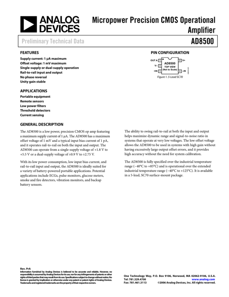
PIN CONFIGURATION
OUT A 1
V– 2
+IN 3
5
V+
4
–IN
AD8500
TOP VIEW
(Not to Scale)
06005-001
Preliminary Technical Data
Micropower Precision CMOS Operational
Amplifier
AD8500
Figure 1. 5-Lead SC70
APPLICATIONS
Portable equipment
Remote sensors
Low power filters
Threshold detectors
Current sensing
GENERAL DESCRIPTION
The AD8500 is a low power, precision CMOS op amp featuring
a maximum supply current of 1 μA. The AD8500 has a maximum
offset voltage of 1 mV and a typical input bias current of 1 pA,
and it operates rail-to-rail on both the input and output. The
AD8500 can operate from a single-supply voltage of +1.8 V to
+5.5 V or a dual-supply voltage of ±0.9 V to ±2.75 V.
The ability to swing rail-to-rail at both the input and output
helps maximize dynamic range and signal-to-noise ratio in
systems that operate at very low voltages. The low offset voltage
allows the AD8500 to be used in systems with high gain without
having excessively large output offset errors, and it provides
high accuracy without the need for system calibration.
With its low power consumption, low input bias current, and
rail-to-rail input and output, the AD8500 is ideally suited for
a variety of battery-powered portable applications. Potential
applications include ECGs, pulse monitors, glucose meters,
smoke and fire detectors, vibration monitors, and backup
battery sensors.
The AD8500 is fully specified over the industrial temperature
range (−40°C to +85°C) and is operational over the extended
industrial temperature range (−40°C to +125°C). It is available
in a 5-lead, SC70 surface-mount package.
Rev. PrA
Information furnished by Analog Devices is believed to be accurate and reliable. However, no
responsibility is assumed by Analog Devices for its use, nor for any infringements of patents or other
rights of third parties that may result from its use. Specifications subject to change without notice. No
license is granted by implication or otherwise under any patent or patent rights of Analog Devices.
Trademarks and registered trademarks are the property of their respective owners.
One Technology Way, P.O. Box 9106, Norwood, MA 02062-9106, U.S.A.
Tel: 781.329.4700
www.analog.com
Fax: 781.461.3113
©2006 Analog Devices, Inc. All rights reserved.
AD8500
Preliminary Technical Data
TABLE OF CONTENTS
Features .............................................................................................. 1
Absolute Maximum Ratings ............................................................5
Applications....................................................................................... 1
Thermal Resistance .......................................................................5
General Description ......................................................................... 1
ESD Caution...................................................................................5
Pin Configuration............................................................................. 1
Outline Dimensions ..........................................................................6
Revision History ............................................................................... 2
Ordering Guide .............................................................................6
Specifications..................................................................................... 3
Electrical Characteristics............................................................. 3
REVISION HISTORY
3/06—PrA: Initial Version
Rev. PrA | Page 2 of 8
Preliminary Technical Data
AD8500
SPECIFICATIONS
ELECTRICAL CHARACTERISTICS
@ VS = +5V, VCM = VS/2, TA = 25°C, unless otherwise noted.
Table 1.
Parameter
INPUT CHARACTERISTICS
Offset Voltage
Offset Voltage Drift
Input Voltage Range
Input Bias Current
Symbol
Conditions
VOS
∆VOS/∆T
0 V < VCM < +5 V
−40°C < TA < +85°C
Min
Typ
Max
Unit
0.235
3
1
10
+5.3
10
100
600
5
50
100
TBD
TBD
mV
μV/°C
V
pA
pA
pA
pA
pA
pA
dB
dB
dB
dB
pF
pF
4.995
4.960
0.85
6.5
±TBD
V
V
mV
mV
mA
−0.3
IB
1
−40°C < TA < +85°C
−40°C < TA < +125°C
Input Offset Current
IOS
Common-Mode Rejection Ratio
CMRR
Large Signal Voltage Gain
AVO
Input Capacitance
CDIFF
CCM
OUTPUT CHARACTERISTICS
Output Voltage High
Output Voltage Low
Short-Circuit Current
POWER SUPPLY
Power Supply Rejection Ratio
Supply Current/Amplifier
DYNAMIC PERFORMANCE
Slew Rate
Gain Bandwidth Product
Phase Margin
NOISE PERFORMANCE
Peak-to-Peak Noise
Voltage Noise Density
Current Noise Density
VOH
VOL
ISC
PSRR
ISY
0.5
−40°C < TA < +85°C
−40°C < TA < +125°C
0 V < VCM < 5 V
−40°C < TA < +85°C
0.1 V < VOUT < 4.9 V
0.1 V < VOUT < 4.9 V; −40°C < TA < +85°C
RLoad = 100 kΩ to GND
RLoad = 10 kΩ to GND
RLoad = 100 kΩ to VS
RLoad = 10 kΩ to VS
VOUT = GND
4.970
4.900
1.8 V < VS < 5 V
−40°C < TA < +85°C
VO = VS/2
−40°C < TA < +85°C
−40°C < TA < +125°C
90
80
SR
GBP
ØO
en
in
75
70
98
80
0.1 Hz to 10 Hz
f = 1 kHz
f = 1 kHz
Rev. PrA | Page 3 of 8
90
90
120
5
15
110
0.75
1
1.5
2
dB
dB
μA
μA
μA
0.004
7
60
V/μs
kHz
Degrees
6
190
TBD
μVp-p
nV/√Hz
fA/√Hz
AD8500
Preliminary Technical Data
@ VS = +1.8V, VCM = VS/2, TA = 25°C, unless otherwise noted.
Table 2.
Parameter
INPUT CHARACTERISTICS
Offset Voltage
Offset Voltage Drift
Input Voltage Range
Input Bias Current
Symbol
Conditions
VOS
∆VOS/∆T
0 V < VCM < +1.8 V
−40°C < TA < +85°C
Min
Typ
Max
Unit
0.235
3.5
1
12
+1.8
10
100
600
5
50
100
TBD
TBD
mV
μV/°C
V
pA
pA
pA
pA
pA
pA
dB
dB
dB
dB
pF
pF
1.798
1.783
V
V
−0.3
IB
1
−40°C < TA < +85°C
−40°C < TA < +125°C
Input Offset Current
IOS
Common-Mode Rejection Ratio
CMRR
Large Signal Voltage Gain
AVO
Input Capacitance
CDIFF
CCM
OUTPUT CHARACTERISTICS
Output Voltage High
Output Voltage Low
Short-Circuit Current
POWER SUPPLY
Power Supply Rejection Ratio
Supply Current/Amplifier
DYNAMIC PERFORMANCE
Slew Rate
Gain Bandwidth Product
Phase Margin
NOISE PERFORMANCE
Peak-to-Peak Noise
Voltage Noise Density
Current Noise Density
0.5
−40°C < TA < +85°C
−40°C < TA < +125°C
0 V < VCM < 1.8 V
−40°C < TA < +85°C
0.1 V < VOUT < 1.7 V
0.1 V < VOUT < 1.7 V; −40°C < TA < +85°C
VOH
RLoad = 100 kΩ to GND
RLoad = 10 kΩ to GND
VOL
RLoad = 100 kΩ to VS
RLoad = 10 kΩ to VS
65
60
88
70
1.790
1.760
0.70
5
±TBD
ISC
PSRR
ISY
1.8 V < VS < 5 V
−40°C < TA < +85°C
VO = VS/2
−40°C < TA < +85°C
−40°C < TA < +125°C
SR
GBP
ØO
en
in
0.1 Hz to 10 Hz
f = 1 kHz
f = 1 kHz
Rev. PrA | Page 4 of 8
85
83
115
90
80
5
15
110
0.65
1
1.5
2
mV
mV
mA
dB
dB
μA
μA
μA
0.004
7
60
V/μs
kHz
Degrees
6
190
TBD
μVp-p
nV/√Hz
fA/√Hz
Preliminary Technical Data
AD8500
ABSOLUTE MAXIMUM RATINGS
TA = 25°C, unless otherwise noted.
Table 3.
Parameter
Supply Voltage
Input Voltage
Differential Input Voltage
Output Short-Circuit Duration to GND
Storage Temperature Range
Lead Temperature (Soldering, 60 sec)
Operating Temperature Range
Junction Temperature Range
Rating
6V
VSS − 0.4 V to VDD + 0.4 V
±6 V
Indefinite
−65°C to +150°C
300°C
−40°C to +125°C
−65°C to +150°C
Stresses above those listed under Absolute Maximum Ratings
may cause permanent damage to the device. This is a stress
rating only; functional operation of the device at these or any
other conditions above those indicated in the operational
section of this specification is not implied. Exposure to absolute
maximum rating conditions for extended periods may affect
device reliability.
Absolute maximum ratings apply at 25°C, unless otherwise
noted.
THERMAL RESISTANCE
θJA is specified for the worst-case conditions, that is, a device
soldered in a circuit board for surface-mount packages.
Table 4. Thermal Characteristics
Package Type
5-Lead SC70 (KS-5)
θJA
376
ESD CAUTION
ESD (electrostatic discharge) sensitive device. Electrostatic charges as high as 4000 V readily accumulate on
the human body and test equipment and can discharge without detection. Although this product features
proprietary ESD protection circuitry, permanent damage may occur on devices subjected to high energy
electrostatic discharges. Therefore, proper ESD precautions are recommended to avoid performance
degradation or loss of functionality.
Rev. PrA | Page 5 of 8
θJC
126
Unit
°C/W
AD8500
Preliminary Technical Data
OUTLINE DIMENSIONS
2.20
2.00
1.80
1.35
1.25
1.15
5
4
1
2
3
2.40
2.10
1.80
PIN 1
0.65 BSC
1.00
0.90
0.70
1.10
0.80
0.10 MAX
0.30
0.15
0.40
0.10
SEATING
PLANE
0.46
0.36
0.26
0.22
0.08
0.10 COPLANARITY
COMPLIANT TO JEDEC STANDARDS MO-203-AA
Figure 2. 5-Lead Thin Shrink Small Outline Transistor Package [SC70]
(KS-5)
Dimensions shown in millimeters
ORDERING GUIDE
Model
AD8500AKSZ-R21
AD8500AKSZ-REEL1
AD8500AKSZ-REEL71
1
Temperature Range
−40°C to +125°C
−40°C to +125°C
−40°C to +125°C
Package Description
5-Lead SC70
5-Lead SC70
5-Lead SC70
Z = Pb-free part.
Rev. PrA | Page 6 of 8
Package Option
KS-5
KS-5
KS-5
Branding
A0F
A0F
A0F
Preliminary Technical Data
AD8500
NOTES
Rev. PrA | Page 7 of 8
AD8500
Preliminary Technical Data
NOTES
©2006 Analog Devices, Inc. All rights reserved. Trademarks and
registered trademarks are the property of their respective owners.
PR06005-0-3/06(PrA)
T
T
Rev. PrA | Page 8 of 8


