AMMP-6220
6-20 GHz Low Noise Amplifier
Data Sheet
Description
Features
Avago’s AMMP-6220 is a high gain, low-noise amplifier that operates from 6 GHz to 20 GHz. The LNA is
designed to be a easy-to-use component for any surface mount PCB application. The broad and unconditionally stable performance makes this LNA ideal for
primary, sub-sequential or driver low noise gain stages. Intended applications include microwave radios,
802.16, automotive radar, VSAT, and satellite receivers.
Since one part can cover several bands, the AMMP-6220
can reduce part inventory and increase volume purchase options. The LNA has integrated 50 W I/O match,
DC blocking, self-bias and choke to eliminate complex
tuning and assembly processes typically required by hybrid (discrete-FET) amplifiers. The package is full SMT
compatible with backside grounding and I/O to simplify
assembly.
• 5x5 mm surface mount package
• Broad Band performance 6-20 GHz
• Low 2.5 dB typical noise figure
• High 22 dB typical gain
•50 W input and output match
• Single 3 V (55 mA) supply bias
• 100% RF test in package
Applications
• Microwave radio systems
• Satellite VSAT
• WLL and MMDS loops
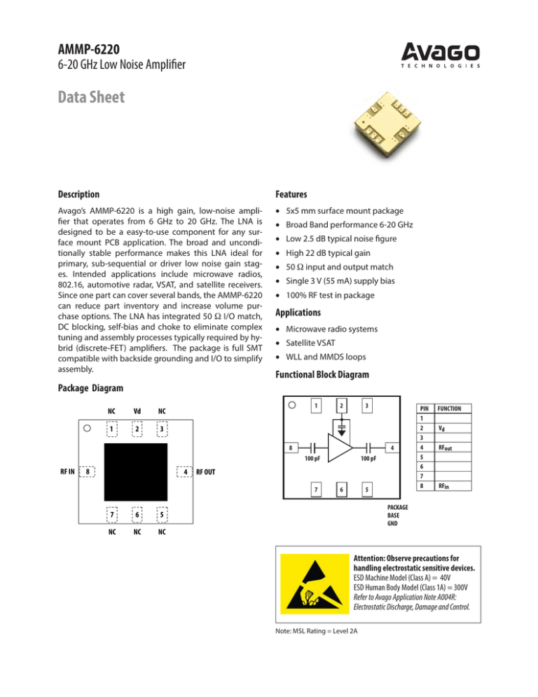
Functional Block Diagram
Package Diagram
NC
Vd
NC
1
2
3
1
2
3
8
4
100 pF
RF IN
8
4
RF OUT
7
7
6
5
NC
NC
NC
100 pF
6
5
PIN
1
2
3
4
5
6
7
8
FUNCTION
Vd
RFout
RFin
PACKAGE
BASE
GND
Attention: Observe precautions for
handling electrostatic sensitive devices.
ESD Machine Model (Class A) = 40V
ESD Human Body Model (Class 1A) = 300V
Refer to Avago Application Note A004R:
Electrostatic Discharge, Damage and Control.
Note: MSL Rating = Level 2A
Electrical Specifications
1. Small/Large -signal data measured in a fully de-embedded test fixture form TA = 25°C.
2. Pre-assembly into package performance verified 100% on-wafer per AMMC-6220 published specifications.
3. This final package part performance is verified by a functional test correlated to actual performance at one or
more frequencies.
4. Specifications are derived from measurements in a 50 W test environment. Aspects of the amplifier performance
may be improved over a more narrow bandwidth by application of additional conjugate, linearity, or low noise
(Гopt) matching.
Table 1. RF Electrical Characteristics
Parameter
Sigma
Unit
Small-signal Gain, Ga
Min
Typ.
22
Max
0.5
dB
Noise Figure into 50 Ω, NF
2.5
0.2
dB
Output Power at 1dB Gain Compression, P-1dB
+10
0.8
dBm
Third Order Intercept Point;
∆f=100MHz; Pin=-20dBm, OIP3
+20
1.1
dBm
Input Return Loss, RLin
-12
0.3
dB
Output Return Loss, Rlout
-16
0.7
dB
Reverse Isolation, Isol
-45
0.5
dB
Table 2. Recommended Operating Range
1. Ambient operational temperature TA = 25°C unless otherwise noted.
2. Channel-to-backside Thermal Resistance (Tchannel (Tc) = 34°C) as measured using infrared microscopy. Thermal
Resistance at backside temperature (Tb) = 25°C calculated from measured data.
Specifications
Description
Min.
Drain Supply Current, Id
Typical
Max.
Unit
Comments
55
70
mA
(Vd = 3 V, Under any RF power drive and
temperature)
Table 3. Thermal Properties
Parameter
Test Conditions
Value
Thermal Resistance, qch-b
qch-b = 27 °C/W
Absolute Minimum and Maximum Ratings
Table 4. Minimum and Maximum Ratings
Specifications
Description
Pin
Max.
Unit
Drain Supply Voltage
Vd
Min.
7
V
Drain Current
Id
100
mA
RF Input Power (Pin)
RFIN
15
dBm
+150
°C
+150
°C
+300
°C
Channel Temperature
Storage Temperature
Maximum Assembly Temperature
-65
Comments
CW
60 second maximum
Notes:
1. Operation in excess of any one of these conditions may result in permanent damage to this device.
2
Selected performance plots
These measurements are in 50Ω test environment at TA = 25°C, Vd = 3V, Id = 55 mA. Aspects of the amplifier performance may be improved over a narrower bandwidth by application of additional conjugate, linearity or low noise
(Γopt) matching.
25
0
-10
-20
15
S21 (dB)
S21 (dB)
20
10
-40
5
0
-30
-50
4
6
10
8
14
16
12
FREQUENCY (GHz)
18
20
-60
22
4
6
8
10
14
16
12
FREQUENCY (GHz)
18
20
22
8
10
14
16
12
FREQUENCY (GHz)
18
20
22
Figure 2. Isolation.
Figure 1. Gain.
0
0
-5
-5
S22 (dB)
S11 (dB)
-10
-10
-15
-20
-15
-25
-20
4
6
10
14
16
12
FREQUENCY (GHz)
8
18
20
-30
22
Figure 3. Input return loss.
4
6
Figure 4. Output return loss.
25
4.0
3.5
20
OP-1dB & OIP3 (dBm)
NF (dB)
3.0
2.5
2.0
1.5
1.0
15
10
P-1dB
5
OIP3
0.5
0
6
8
Figure 5. Noise figure.
3
10
14
16
12
FREQUENCY (GHz)
18
20
0
6
8
10
14
12
FREQUENCY (GHz)
Figure 6. Typical power, OP-1dB and OIP3.
16
18
20
Over Temperature Performance Plots
These measurements are in 50Ω test environment at TA = 25°C, Vd = 3V, Id = 55 mA. Aspects of the amplifier performance may be improved over a narrower bandwidth by application of additional conjugate, linearity or low noise
(Γopt) matching.
30
0
25
-10
20
-20
+25C
S12 (dB)
S21 (dB)
-40C
15
+25C
10
+85C
-30
-40
-40C
5
0
-50
+85C
4
6
8
10
16
12
14
FREQUENCY (GHz)
18
20
-60
22
4
6
8
10
16
14
12
FREQUENCY (GHz)
18
20
22
20
22
Figure 8. Isolation over temperature.
Figure 7. Gain over temperature.
0
0
+25C
+25C
-5
+85C
-10
S22 (dB)
+85C
S11 (dB)
-40C
-40C
-5
-10
-15
-20
-15
-25
-20
4
6
10
8
14
16
12
FREQUENCY (GHz)
18
20
Figure 9. Input return loss over temperature.
4.0
6
8
10
16
14
12
FREQUENCY (GHz)
18
62
+25C
-40C
3.0
4
Figure 10. Output return loss over temperature.
+25C
3.5
-40C
60
+85C
+85C
58
Idd (mA)
2.5
NF (dB)
-30
22
2.0
1.5
56
54
1.0
52
0.5
0
6
8
10
14
12
FREQUENCY (GHz)
Figure 11. NF over temperature.
4
16
18
20
50
3.0
3.5
4.0
Vdd (V)
Figure 12. Bias current over temperature.
4.5
5.0
Over Voltage plots
These measurements are in 50Ω test environment at TA = 25°C, Vd = 3V, Id = 55 mA. Aspects of the amplifier performance may be improved over a narrower bandwidth by application of additional conjugate, linearity or low noise
(Γopt) matching.
25
0
S12 (dB)
S21 (dB)
10
5V
4V
5
-50
5V
4
6
10
8
14
16
12
FREQUENCY (GHz)
18
20
-30
-40
3V
-60
22
Figure 13. Gain over Vdd.
4
6
10
8
14
16
12
FREQUENCY (GHz)
18
20
22
18
20
22
Figure 14. Isolation over Vdd.
0
0
3V
3V
4V
-5
4V
-5
5V
5V
-10
S22 (dB)
S11 (dB)
4V
-20
15
0
3V
-10
20
-10
-15
-20
-15
-25
-20
4
6
10
8
14
16
12
FREQUENCY (GHz)
18
20
Figure 15. Input RL over Vdd.
3.0
25
2.5
20
OIP3 (dBm)
NF (dB)
1.5
3V
1.0
0.5
8
10
12
14
FREQUENCY (GHz)
Figure 17. Noise figure over Vdd.
10
8
14
16
12
FREQUENCY (GHz)
16
18
15
10
3V
5V
5
5V
6
6
4V
4V
0
4
Figure 16. Output return loss over temperature.
2.0
5
-30
22
20
0
6
8
10
Figure 18. OIP3 over Vdd.
14
16
12
FREQUENCY (GHz)
18
20
Biasing and Operation
The AMMC-6220 is normally biased with a single positive
drain supply connected to both VD pin through bypass
capacitors as shown in Figure 19. The recommended
supply voltage is 3 V. It is important to have 0.1 µF bypass
capacitor, and the capacitor should be placed as close to
the component as possible.
The AMMC-6220 does not require a negative gate voltage
to bias any of the three stages. No ground wires are
needed because all ground connections are made with
plated through-holes to the backside of the package.
Refer the Absolute Maximum Ratings table for allowed
DC and thermal conditions.
Application Circuit
VD (TYP. 3 V)
1
0.1 µF
2
3
RFin
RFout
8
4
100 pF
7
100 pF
6
5
PACKAGE
BASE
GND
Figure 19. Typical application
Figure 21. Demonstration board (available upon request)
VD
RFout
RFin
Figure 20. Simplified MMIC schematic
6
Typical Scattering Parameters
Please refer to <http://www.avagotech.com> for typical scattering parameters data.
Package Dimension, PCB Layout and Tape and Reel information
Please refer to Avago Technologies Application Note 5520, AMxP-xxxx production Assembly Process (Land Pattern A).
AMMP-6220 Part Number Ordering Information
Part Number
Devices Per Container
Container
AMMP-6220-BLK
10
Antistatic bag
AMMP-6220-TR1
100
7” Reel
AMMP-6220-TR2
500
7” Reel
For product information and a complete list of distributors, please go to our website:
www.avagotech.com
Avago, Avago Technologies, and the A logo are trademarks of Avago Technologies in the United States and other countries.
Data subject to change. Copyright © 2005-2013 Avago Technologies. All rights reserved. Obsoletes 5989-4517EN
AV02-0515EN - July 9, 2013
