An improved junction field-effect transistor static model for integrated
advertisement
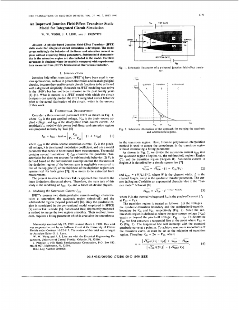
IEEE TRANSACTIONS ON ELECTRON DEVICES. VOL. 37. NO. 7. JULY I990 I773 +- An Improved Junction Field-Eff ect Transistor Static Model for Integrated Circuit Simulation I I W. W. WONG. J . J . LIOU, A N D J. PRENTICE Abstract-A physics-based Junction Field-Effect Transistor (JFET) static model for integrated circuit simulation is developed. The model covers unifyingly the behavior of the linear and saturation current regions without requiring fitting parameters. Subthreshold characteristics in the saturation region are also included in the model. Excellent agreement is obtained when the model is compared with experimental data measured from JFET’s fabricated at Harris Semiconductor. I I I I I BOTTOM GATE -+--- VSO Fig. 1. Schematic illustration of a p-channel junction field-effect transistor. I. INTRODUCTION Junction field-effect transistors (JFET’s) have been used in various applications, such as in power electronics and in analog/digital circuits, because they enable certain circuit functions to be achieved with a degree of simplicity. Research on JFET modeling was active in the 1960’s but has not been extensive in the past twenty years [I]-[4]. What is needed is a JFET model with which the circuit designers can quickly predict the JFET integrated circuit behavior prior to the actual fabrication of the circuit, which is the essence of this work. 11. THEORETICAL DEVELOPMENT Consider a three-terminal p-channel JFET as shown in Fig. I , where VGs is the gate applied voltage, VsD is the drain-source applied voltage, and IsD is the steady-state drain-source current. An empirical IsD model which covers both linear and saturation regions was proposed recently by Taki [5] where IsDs is the drain-source saturation current, V p is the pinchoff voltage, X is the channel modulation coefficient, and CY is a model parameter that needs to be extracted from measurement. The model contains several limitations: 1) IsDs considers the quadratic characteristics but does not account for subthreshold behavior; 2) V p is derived based on the conventional assumption that the thickness of the depletion region of the bottom gate is negligible compared to that of the top gate [6] or the thickness of the depletion regions are symmetrical for both gates [ 7 ] ; 3) a needs to be extracted from measurement. The present treatment follows Taki’s approach but removes the three limitations discussed above. Therefore, the main task of this study is the modeling of IsDs. V p , and CY based on device physics. ~ , ‘= - 1 quadratic I \ i I transition subthreshold I Fig. 2. Schematic illustration of the approach for merging the quadratic and subthreshold regions. in the transition region. Here, Hermite polynomial-interpolation method is used to assure the smoothness in the transition region without introducing a fitting parameter. As shown in Fig. 2, we divide the saturation current IsDs into the quadratic region (Region A ) , the subthreshold region (Region C ) , and the transition region (Region B). Saturation current in Region A is described by a simple square law [7] and Ism= ( W / L ) p V ; , where W is the channel width, L is the channel length, and 0 is the quadratic transfer parameter. The current in Region C exhibits an exponential character due to the “barrier mode” behavior [8] CS = JI,, . e ( - l v < T 5 - v P l ) / v ! A. Modeling the Saturation Current IsDs JFET’s possess two distinguishable current-voltage characteristics at saturation: the quadratic region (pinch-off) and the subthreshold region (beyond pinch-off) [8]. Only the quadratic region is considered in the conventional model employed in SPICE [9] and in Taki’s model [ 5 ] . Sansen and Das [IO] recently proposed a method to merge the two regions smoothly. Their method, however, requires a fitting parameter which is crucial to the smoothness Manuscript received July 27, 1989; revised March 8, 1990. This work was supported in part by an In-House Grant at the University of Central Florida under Contract 16-22-917. The review of this brief was arranged by Associate Editor S . E. Laux. W. W. Wong and J. J. Liou are with the Electrical Engineering Department, University of Central Florida, Orlando, FL 32816. J . Prentice is with Harris Semiconductor Corporation. P.O. Box 883. MS 58-007, Melbourne, FL 32901. IEEE Log Number 9036008. (3) where V, is the thermal voltage and Iop is the pinch-off current (I, at VGs = V p ) . The transition region is treated as follows. Let the voltages the quadratic-transition boundary and the subthreshold-transitic boundary be V B l and VBz, respectively (Fig. 2 ) . Since the subthreshold region is defined as where the gate-source voltage ( VGs) equals or beyond the pinch-off voltage, VB2 - V,. To determine V B , , we first construct a tangential line at the point where VGs = V p (Fig. 2). The tangential line will intercept with the extended quadratic curve at a point m . To achieve maximum smoothness of the transition curve, m must be set as the midpoint of transition region. Therefore V B l = 2m - VBz,where 0018-9383/90/0700-1773$01 .OO 0 1990 IEEE [ 1774 I E E E TRANSACTIONS ON ELECTRON DEVICES. VOL. 37. NO. 7. J U L Y I9YU Putting the boundary conditions into Hermite interpolation equation yields [ l l ] JG= 4 1 - VBIiVP) [ ’ - 2(VGS - 2 . [(VGS + - VBl)iV8121 V,’)/V,l’l’ JI,,exp [ ( V P - V,2)/2V,] . [I - 2(VGS - VSl)/VBI?] [ ( V G S - (Jlsoo/VP)(VGS - ( G P / 2 V , ) exp - V,I)[(VGS [(VP - - ~Bl)/~€Jl’l~ - VB2)/VB12I2 V82)/2V,][(VGS- ~BI)/VBI*l’ (5) where Vslz = VsI - V,?. We next proceed to develop expressions for the pinch-off voltage V p and the quadratic transfer parameter 0 required in (5). I ) Pinch-Of Voltage Vp: The top-gate and bottom-gate depletion thickness ( X T and X , ) can be obtained from the conventional depletion model [ 1 2 ] . When pinch-off occurs at x = L , VGS becomes V p and h = X T p + X B p , where X r p and X,, are X T and X , at pinch-off. Thus Fig. 3. Schematic illustration of the approach for modeling (Y drain current IsoA at VA (Fig. 3), then substituting the model into ( I ) , we have a =2 . tanh-’ I 2 . (3 - 2hVp) ( 2 - AVp$ J (9) The values of calculated and measured a for three JFET’s are given in Table I. Kl = NDT/[NA ’ (NA + NDT)] and K? = N D 8 / [ N A ’ ( N A + where is the dielectric permittivity, $T and $, are the top- and bottom-gate junction built-in potentials, and NDrr N A , and N,, are the doping concentrations in the top-gate, the channel, and the bottom-gate, respectively. Solving for V p in ( 6 ) , we get Vp = [ (B’ - 2 A C ) / 2 A 2 ] - ( 1 / 2 A ’ ) . [ ( 2 A C - B’)’ A = Kl B = - - 4A’( C’ - B’$,)]”’ C . Channel Length Modulation Coe@cient X When VS, is increased exceeding the saturation source-drain voltage, the conduction channel length is shortened because of the overlap of the top and bottom depletion regions. As a consequence, the source-drain current may increase slightly with the increase of VSo. This results in a channel length modulation coefficient X which can be expressed as x = (7) K2 h (2qK?/~,,)().’ and C = -qh’/2 + ~ T K-I $EK?. 2 ) Quadratic Transfer Parameter (3: According to Grove 1131, CL the channel conductance gSo equals the channel transconductance g,,, of a JFET. Equating g,s, and g,,, and setting VG,s= 0 yields where H is the average undepleted channel height and p,, is the hole mobility. B. Modeling a Basically, a can be obtained from ( I ) by letting VGS = 0 and by selecting a Vsu at which ISD can be found. Taki [ 5 ] selects VSD= V p and obtains Is, at Vp from experimental data, from which he determines a . Here we model ct without requiring measurement. First, tangential lines at VSo = 0 and at VSD> VsDs(drain-source saturation voltage) are constructed based on the conventional JFET linear and saturation models [ 7 ] , [9] at VGS = 0 (Fig. 3). The two lines intersect at VsD = VA (Fig. 3). which is found to be V, = V p / (2 - A V p ) . Because the value of X is normally in the range of 0.001 to 0.01, AVp is negligible compared to 2 . Therefore, VA = V p / 2 , which falls into the linear region. Replacing VSDby VA in the conventional JFET linear model 171. 191. which results in the = AL/(LV~,) (10) where A L is the overlap dep1etion:region length, which is conventionally modeled as [ 141 A[(26s,/qNA)(VSD + ‘GS - ‘P)] ”’ (11) where A is an empirical parameter; A = I for long-channel JFET’s and A > 1 for short-channel JFET’s. 111. ILLUSTRATION AND CONCLUSION In support of the model, we have obtained experimental data from JFET’s fabricated at Harris Semiconductor (devices’ makeup and measured and calculated devices’ parameters are summarized in Table I). Fig. 4 illustrates the comparison of the saturation drain current versus the gate voltage calculated from the present model (solid line) and obtained from measurement (closed circles). Sensitivity analysis is also carried out by varying the device geometry & 5 % (error bars), which corresponds a typical process tolerance. It is shown that Hermite interpolation indeed links the quadratic and subthreshold regions smoothly and continuously. Fig. 5 illustrates the drain current versus the drain-source voltage characteristics as a function of the gate voltage (step). In conclusion, we have developed an accurate and physics-based three-terminal JFET static model for circuit simulation. The present model has several advantages over the conventional JFET model used in SPICE: I ) The JFET model in SPICE requires two different models for the linear and saturation regions whereas the present model treats both regions unifyingly without introducing fitting parameters. 2 ) The JFET model in SPICE neglects the subthreshold behavior whereas the present model includes such effects. 3) The JFET model in SPICE requires several model parameters that need to be extracted from measurements whereas the present model requires only the device makeup, such as the doping concentrations and the junction depths, which can be obtained from process simulators such as SUPREM. I775 IEEE TRANSACTIONS ON ELECTRON DEVICES. VOL. 37. NO. 7. JULY 1990 TABLE I DEVICE’ JFETl JPETZ vp (VI W/L (pm/pm) mea. 200/25 cal. JI, mea. JI,, (lO.’JA) mea. cal. (1O-’JA) cal. 1.95 1.96 2.14 1.97 1.98 2.03 Device channel height: 0 . 2 (pm) . Device doping concentration: N, =9*10l6 ( ~ r n - ~:) NOB = 10‘’ ( ~ m -:~and ) N,, = 1.3*10” (cm-’) 1.7 1.8 1.9 200/15 200/10 1.8 1.8 1.8 1.0 1.5 2.0 - model 11I sensctmfv a n w i s e e e 17.8 24.0 29.5 cal. 18.1 23.3 28.6 JFET3 1.8 2.4 3.1 a mea. IIIsensrtivii anaiysis 0 measurement OW measurement 100 200 300 ,v Fig. 4. Saturation current lsuscalculated from the present model (solid line), obtained from measurement (closed circles). and calculated from the present model by varying the device geometry f5% (error bars) for three JFET’s. REFERENCES R. S. C. Cobbold, Theory and Applicution of Field-Efect Trunsistors. New York, NY: Wiley, 1970. F. A. Lindholm and P. R. Gray. “Large-signal and small-signal models for arbitrarily doped four-terminal field-effect transistors,” IEEE Trunu. Electron Devices, vol. ED-13, pp. 819-829, Dec. 1966. P. H. Hudson. F. A . Lindholm, and D. J. Hamilton, “Transient performance of four-terminal field-effect transistors,” IEEE Truns. Electron Devices. vol. ED-12. pp. 399-407, July 1965. R. S . C. Cobbold and F. N. Trofimenkoff, “Four-terminal field-effect transistors.” IEEE Truns. Electron Devices, vol. ED-12. pp. 246- 247. May 1965. T. Taki, “Approximation of junction field-effect transistor characteristics by a hyperbolic function.” IEEE J. Solid-Stute Circuits. vol. SC-13. Oct. 1978. R. S. Muller and T. I. Kamins, Device Electronics f . r Intrgrured Circuits. 2nd ed. New York, NY: Wiley, 1986. . 400 500 600 700 800 (volts) Fig. 5 . I.\/]versus VFI)characteristics calculated from the present model (solid lines), obtained from measurement (closed circles), and calculated from the present model by varying the device geometry + 5 % (error bars). 171 S. M. Sze, Physics of Semiconductor Devices, 2nd ed. New York, NY: Wiley. 1981. (81 R . J . Brewer, “The ‘barrier mode’ behavior o f a junction FET at low drain currents,” Solid-Stute Electron., vol. 18, pp. 1013-1017, 1975. 191 P. Antognetti and G. Massobrio, Semiconcluctor Device Modeling with SPICE. New York, NY: McGraw-Hill. 1988. [IO] W. M. Sansen and C. J. M. Dw. “A simple model for ion-implanted JFET’s valid in both the quadratic and the subthreshold regions,” IEEE J. Solid-Stutr Circuits, vol. SC-17, pp. 658-666, 1982. [ I I ] R. L. Burden and J. D. Fakes. Numericul Anulysis, 3rd ed. Boston. MA: PWS Publishers, 1985. [ 121 H. Shichman and D. A. Hodges. “Modeling and simulation of insulated-gate field-effect transistor switching circuit,” IEEE J. SolidStutr Circuits, vol. SC-3, 1968. [ 131 A. S . Grove. Physics und Technology of Semiconductor Devices. New York, N Y : Wiley, 1967, p. 252. [ 141 C. D. Hartgring, “ A n accurate JFETlMESFET model for circuit analysis,” Solid-Stute Electron.. vol. 25, pp. 233-240. 1982.
