1.5A,2.3V-6V Input,1.5MHz
Synchronous Step-Down Converter
CASC
FEATURES
GENERAL DESCRIPTION
High Efficiency: Up to 96%
1.5MHz Constant Frequency Operation
1.5A Output Current
No Schottky Diode Required
2.3V to 6V Input Voltage Range
Adjustable Output Voltage Range Options
from 0.6V to V IN
100% Duty Cycle in Dropout Operation
Low Quiescent Current: 35μA
Slope Compensated Current Mode Control for
Excellent Line and Load Transient Response
Short Circuit Protection
Thermal Fault Protection
Inrush Current Limit and Soft Start
<1μA Shutdown Current
SOT23-5 package
MT3410
AEROSEMI
APPLICATIONS
The MT3410 is high-efficiency,high frequency
synchronous step-down DC-DC regulator ICs
capable of delivering up to 1.5A output
currents.The MT3410 can operate over a wide
input voltage range from 2.3V to 6V and integrates
main switch and synchronous switch with very
low R DS(ON) to minimize the conduction loss.
It is ideal for powering portable equipment that
runs from a single cell Lithium-Ion(Li+)
battery.The output voltage can be regulated as low
as 0.6V.The MT3410 can also run at 100% duty
cycle for low dropout operation,extending battery
life in portable system.This device offers two
operation modes,PWM mode and PFM mode
switching control,which allows a high efficiency
over the wide range of the load.
The MT3410 is offered in a low profile 5-pin SOT
package,and is available in an adjustable version.
Cellular and Smart Phones
Wireless and DSL Modems
PDAs
Portable Instruments
Digital Still and Video Cameras
Set Top Box
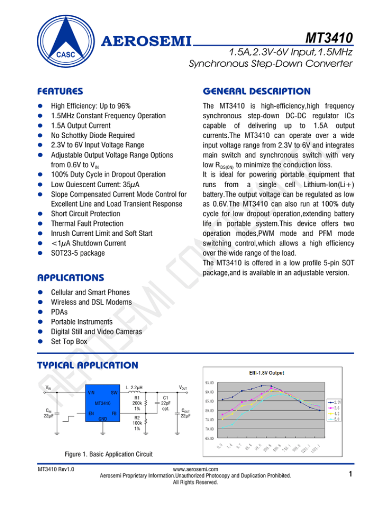
TYPICAL APPLICATION
VIN
VIN
SW
MT3410
CIN
22μF
EN
GND
FB
VOUT
L 2.2μH
R1
200k
1%
R2
100k
1%
C1
22pF
opt.
COUT
22μF
Figure 1. Basic Application Circuit
MT3410 Rev1.0
www.aerosemi.com
Aerosemi Proprietary Information.Unauthorized Photocopy and Duplication Prohibited.
All Rights Reserved.
1
AEROSEMI
MT3410 1.5A ,1.5MHz Synchronous Step-Down Converter
ABSOLUTE MAXIMUM RATINGS (Note 1)
Input Supply Voltage………………-0.3V to 6.5V
EN,FB Voltages…………….-0.3V to (V IN +0.3V)
SW Voltage………………...-0.3V to (V IN +0.3V)
Power Dissipation………………………...0.4W
Thermal Resistance θ JC ………………..130°C/W
Thermal Resistance θ JA ………………..250°C/W
Junction Temperature(Note2)…………….150°C
Operating Temperature Range…….-40°C to 85°C
Lead Temperature(Soldering,10s)………...300°C
Storage Temperature Range……..-65°C to 150°C
ESD HBM(Human Body Mode)……………...2kV
ESD MM(Machine Mode)………………….200V
PACKAGE/ORDER INFORMATION
Order Part Number
Package
Top Marking
MT3410
SOT23-5
AS15DW
TOP VIEW
EN
1
GND
2
SW
3
5
FB
4
VIN
5-LEAD PLASTIC SOT-23
TJMAX = 150°C, θJA = 250°C/ W, θJC = 130°C/W
PIN DESCRIPTION
Pin Name
Pin Number
EN
1
GND
2
SW
3
VIN
4
FB
5
MT3410 Rev1.0
Description
Chip Enable Pin. Drive EN above 1.5V to turn on the part. Drive EN below
0.3V to turn it off. Do not leave EN floating.
Analog ground pin.
Power Switch Output. It is the switch node connection to Inductor. This
pin connects to the drains of the internal P-ch and N-ch MOSFET
switches.
Power Supply Input.Must be closely decoupled to GND with a 10µF or
greater ceramic capacitor.
Output Voltage Feedback Pin. An internal resistive divider divides the
output voltage down for comparison to the internal reference voltage.
www.aerosemi.com
Aerosemi Proprietary Information.Unauthorized Photocopy and Duplication Prohibited.
All Rights Reserved.
2
AEROSEMI
MT3410 1.5A ,1.5MHz Synchronous Step-Down Converter
ELECTRICAL CHARACTERISTICS (Note 3)
(V IN =V E N =3.6V, V OUT =1.8V, T A = 25°C, unless otherwise noted.)
PARAMETER
CONDITIONS
MIN
Input Voltage Range
2.3
UVLO Threshold
1.7
Input DC Supply Current
(Note 4)
PWM Mode
V OUT = 90%, I LOAD =0mA
PFM Mode
V OUT = 105%, I LOAD =0mA
Shutdown Mode
V EN = 0V, V IN =4.2V
T A = 25°C
0.588
Regulated Feedback
T A = 0°C ≤T A ≤85°C
0.586
Voltage V FB
T A = -40°C ≤T A ≤85°C
0.585
Reference Voltage Line
V IN =2.5V to 6V
Regulation
Output Voltage Line
V IN =2.5V to 6V
Regulation
Output Voltage Load
Regulation
V OUT =100%
Oscillation Frequency
V OUT =0V
On Resistance of PMOS
I SW =100mA
On Resistance of NMOS
I SW =-100mA
Peak Current Limit
V IN = 3V, V OUT =90%
EN Threshold
0.30
EN Leakage Current
SW Leakage Current
V EN =0V,V IN =V SW =5V
TYP
1.9
MAX
6
2.1
140
35
0.1
0.600
0.600
0.600
300
70
1.0
0.612
0.613
0.615
UNIT
V
V
µA
µA
µA
µA
V
V
V
0.04
0.40
%/V
0.04
0.40
%
0.5
%
1.5
300
130
100
2.5
1.0
±0.01
±0.01
MHz
kHz
mΩ
mΩ
A
V
µA
µA
200
200
1.50
±1.0
±1.0
Note 1: Absolute Maximum Ratings are those values beyond which the life of a device may be impaired.
Note 2: T J is calculated from the ambient temperature T A and power dissipation P D according to the
following formula: T J = T A + (P D ) x (250°C/W).
Note 3: 100% production test at +25°C. Specifications over the temperature range are guaranteed by
design and characterization.
Note 4: Dynamic supply current is higher due to the gate charge being delivered at the switching
frequency.
MT3410 Rev1.0
www.aerosemi.com
Aerosemi Proprietary Information.Unauthorized Photocopy and Duplication Prohibited.
All Rights Reserved.
3
AEROSEMI
MT3410 1.5A ,1.5MHz Synchronous Step-Down Converter
TYPICAL PERFORMANCE CHARACTERISTICS
PFM MODE
MT3410 Rev1.0
www.aerosemi.com
Aerosemi Proprietary Information.Unauthorized Photocopy and Duplication Prohibited.
All Rights Reserved.
4
AEROSEMI
MT3410 1.5A ,1.5MHz Synchronous Step-Down Converter
FUNCTIONAL BLOCK DIAGRAM
EN
VIN
RS
OSC &
Shutdown
Control
Current Limit
Detector
Slope
Compensation
PWM/PFM
Mode
Detector
Current
Sensor
FB
Error
Amplifier
PWM
Compartor
Control Logic
Driver
Zero Detector
SW
GND
UVLO & Power
Good Detector
VREF
Figure 2. MT3410 Block Diagram
FUNCTIONAL DESCRIPTION
MT3410 is a synchronous buck regulator IC that
integrates the PWM/PFM control, high-side and
low-side MOSFETs on the same die to minimize
the switching transition loss and conduction loss.
With ultra low R DS(ON) power switches and
proprietary PWM control, this regulator IC can
achieve the highest efficiency and the highest
switch frequency simultaneously to minimize the
external inductor and capacitor size, and thus
achieving the minimum solution footprint. The
MT3410 requires only three external power
components (C IN ,C OUT and L).The adjustable
MT3410 Rev1.0
version can be programmed with external
feedback to any voltage, ranging from 0.6V to
the input voltage. At dropout operation, the
converter duty cycle increases to 100% and the
output voltage tracks the input voltage minus the
R DS(ON) drop of the high-side MOSFET. The
internal error amplifier and compensation
provides excellent transient response, load and
line regulation. Soft start function prevents input
inrush current and output overshoot during start
up.
www.aerosemi.com
Aerosemi Proprietary Information.Unauthorized Photocopy and Duplication Prohibited.
All Rights Reserved.
5
AEROSEMI
MT3410 1.5A ,1.5MHz Synchronous Step-Down Converter
APPLICATIONS INFORMATION
Setting the Output Voltage
The internal reference V REF is 0.6V(Typical).The
output voltage is divided by a resistor,R1 and R2
to the FB pin. The output voltage is given by:
R1
VOUT = 0.6 × 1 +
R2
Inductor Selection
For most designs, the MT3410 operates with
inductors of 1µH to 4.7µH. Low inductance
values are physically smaller but require faster
switching, which results in some efficiency loss.
The inductor value can be derived from the
following equation:
L=
VOUT × (VIN − VOUT )
VIN × ΔIL × fOSC
Where ΔI L is inductor Ripple Current. Large
value inductors result in lower ripple current and
small value inductors result in high ripple current.
For optimum voltage-positioning load transients,
choose an inductor with DC series resistance in
the 50mΩ to 150mΩ range.
Input Capacitor Selection
With the maximum load current at 1.5A,the
maximum ripple current through input capacitor
is about 0.6Arms.A typical X7R or better grade
ceramic capacitor with 6V rating and greater than
10μF capacitance can handle this ripple current
well. To minimize the potential noise problem,
place this ceramic capacitor really close to VIN
and GND pins. Care should be taken to minimize
the loop area formed by C IN , and VIN/GND pins.
Output Capacitor Selection
The output capacitor is required to keep the
output voltage ripple small and to ensure
regulation loop stability. The output capacitor
must have low impedance at the switching
frequency. Ceramic capacitors with X5R or X7R
dielectrics are recommended due to their low
ESR and high ripple current ratings. The output
ripple ΔV OUT is determined by:
ΔVOUT ≤
VOUT × (VIN − VOUT )
1
× ESR +
VIN × fOSC × L
8 × fOSC × C OUT
A 10µF ceramic can satisfy most applications.
PCB Layout Recommendations
When laying out the printed circuit board, the
following checking should be used to ensure
proper operation of the MT3410. Check the
following in your layout:
The power traces, consisting of the GND
trace, the SW trace and the VIN trace should
be kept short, direct and wide
Does the (+) plates of C IN connect to VIN as
closely as possible. This capacitor provides
the AC current to the internal power
MOSFETs.
Keep the switching node, SW, away from
the sensitive V OUT node.
Keep the (-) plates of C IN and C OUT as close
as possible
VIA TO VOUT
R1
VIA TO VIN
C1
PIN1
GND
CIN
COUT
VOUT
R2
MT3410
L
SW
VIN
Figure 3. MT3410 Suggested Layout
MT3410 Rev1.0
www.aerosemi.com
Aerosemi Proprietary Information.Unauthorized Photocopy and Duplication Prohibited.
All Rights Reserved.
6
AEROSEMI
MT3410 1.5A ,1.5MHz Synchronous Step-Down Converter
PACKAGE DESCRIPTION
SOT23-5
e1
5LD SOT-23 PACKAGE OUTLINE DIMENSIONS
Dimension
A
A1
B
C
D
H
E
e
e1
L1
L
Q
EXAMPLE
TOP MARK
AAAA
E
H
PIN 1
Min.
1.05
0.04
0.3
0.09
2.8
2.5
1.5
Max.
1.35
0.15
0.5
0.2
3.0
3.1
1.7
0.95 REF.
1.90 REF.
0.2
0.35
0°
0.55
0.8
10°
TOP VIEW
D
L
A
SEATING PLANE
B
e
A1
FRONT VIEW
Q
L1
C
SIDE VIEW
NOTE:
1.DIMENSIONS ARE IN MILLIMETERS
2.DRAWING NOT TO SCALE
3.DIMENSIONS ARE INCLUSIVE OF PLATING
4.DIMENSIONS ARE EXCLUSIVE OF MOLD FLASH AND METAL BURR
MT3410 Rev1.0
www.aerosemi.com
Aerosemi Proprietary Information.Unauthorized Photocopy and Duplication Prohibited.
All Rights Reserved.
7
AEROSEMI
MT3410 1.5A ,1.5MHz Synchronous Step-Down Converter
IMPORTANT NOTICE
Xi’an Aerosemi Technology Co.,Ltd reserve the right to make corrections, enhancements, improvements
and other changes to its semiconductor products and services.
Xi’an Aerosemi Technology Co.,Ltd is not responsible or liable for such altered documentation. Information
of third parties may be subject to additional restrictions.
Xi’an Aerosemi Technology Co.,Ltd does not assume any responsibility for use of any its products for any
particular purpose, nor does Xi’an Aerosemi Technology Co.,Ltd assume any liability arising out of the
application or use of any its products or circuits.
MT3410 Rev1.0
www.aerosemi.com
Aerosemi Proprietary Information.Unauthorized Photocopy and Duplication Prohibited.
All Rights Reserved.
8


