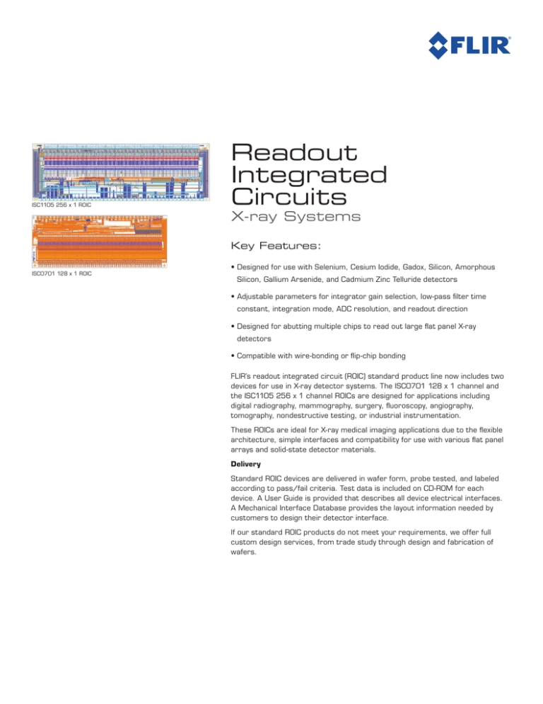
ISC1105 256 x 1 ROIC
Readout
Integrated
Circuits
X-ray Systems
Key Features:
ISC0701 128 x 1 ROIC
• Designed for use with Selenium, Cesium Iodide, Gadox, Silicon, Amorphous
Silicon, Gallium Arsenide, and Cadmium Zinc Telluride detectors
• Adjustable parameters for integrator gain selection, low-pass filter time
constant, integration mode, ADC resolution, and readout direction
• Designed for abutting multiple chips to read out large flat panel X-ray
detectors
• Compatible with wire-bonding or flip-chip bonding
FLIR’s readout integrated circuit (ROIC) standard product line now includes two
devices for use in X-ray detector systems. The ISC0701 128 x 1 channel and
the ISC1105 256 x 1 channel ROICs are designed for applications including
digital radiography, mammography, surgery, fluoroscopy, angiography,
tomography, nondestructive testing, or industrial instrumentation.
These ROICs are ideal for X-ray medical imaging applications due to the flexible
architecture, simple interfaces and compatibility for use with various flat panel
arrays and solid-state detector materials.
Delivery
Standard ROIC devices are delivered in wafer form, probe tested, and labeled
according to pass/fail criteria. Test data is included on CD-ROM for each
device. A User Guide is provided that describes all device electrical interfaces.
A Mechanical Interface Database provides the layout information needed by
customers to design their detector interface.
If our standard ROIC products do not meet your requirements, we offer full
custom design services, from trade study through design and fabrication of
wafers.
Specifications
ROIC Parameter
Input DC Offset
ISC0701
128 x 1 Specification
1.0 to 3.5 V (nominal 1.2 V)
ISC1105
1.0 to 2.6 V (nominal 1.2 V)
Carrier Collected
Electrons
Electrons, Holes
Input Charge Handling
(Normal operation)
≥ 15 pC
≥ 15 pC
Input Charge Handling
(Reset)
≥ 200 pC
≥ 200 pC
Readout Noise
ENC
≤ 800 e- (CINT = 0.25 pF, CDET = 30 pF,
ΔVINT = 1.5 V, tau = 3.7 µs, 13 bit)
ENC
≤ 500 e- (CINT = 0.25 pF, CDET = 50 pF,
ΔVINT = 2 V, tau = 5.2 µs, 16 bit)
Readout Noise
ENC
ENC
≤ 3000 e- (CINT = 4.00 pF, CDET = 30 pF, ≤ 5000 e- (CINT = 8.00 pF, CDET = 50 pF,
ΔVINT = 4 V, tau = 5.0 µs, 14 bit)
ΔVINT = 2 V, tau = 5.2 µs, 16 bit)
Integrator Gain
Control
CINT = 0.25 pF – 4.0 pF,
0.25 pF increments
LPF Time Constant
1 µs, 2.3 µs, 3.7 µs, 5 µs ±20%
1.2 µs – 11 µs ±30%, 3 bits, ~1.4 µs/step
≤ 0.5%
≤ 0.25%
PSRR
≥ 30 dB at ≤ 400 Hz
≥ 40 dB at ≤ 250 Hz
# Of Channels
128
256
Channel Pitch
80 µm
50 µm
ADC Resolution
12, 13, 14 bits
12 - 16 bits
Operating Temperature 10°C – 70°C
10°C – 70°C
Power Dissipation
≤ 1.5 mW/channel – default
≤ 3.0 mW/channel – max front end
≤ 0.1 mW/channel – sleep mode
Clock Frequency
85 MHz
128 MHz
Minimum Line Time
69 µs (12 bit ADC)
83 µs (13 bit ADC)
250 µs (14 bit ADC)
18 µs (12 bit ADC)
34 µs (13 bit ADC)
66 µs (14 bit ADC)
130 µs (15 bit ADC)
258 µs (16 bit ADC)
Input Biases
VPOS
VNEG
VPOSR
VNEGR
VNEGADC
VPOSD
VPD
VND
VREF_INT
5.5 V
0.0 V
5.5 V
0.0 V
0.0 V
5.5 V
3.3 V / 2.5 V
0.0 V
1.2 V (nom)
VREF_CDS
0.5 V (nom)
VREF_ADC
VREF_RAMP
0.5 V (nom)
4.5 V (nom)
VPOS, VPOSINT
VNEG, VNEGINT
VPOSR
VNEGR
VNEGADC
VPOSD
VPD
VND
VREF_INT
VREF_CDS
VREF_ADC
VREF_RAMP
Input Clocks
Name
VIC
CLK
SYNC
DATA
1.25 V
1.25 V
1.25 V
VID
0.35 V
0.35 V
0.35 V
Adjustable integrator DC operating point
Does not include system or detector contributions
CINT = 0.25 pF – 8.0 pF,
0.25 pF increments, FSC= 0.5 pC – 16 pC
ROIC Crosstalk
≤ 1.4 mW/channel
Comments
256 x 1 Specification
Name
CLK
SYNC
DATA
INJCLK
At ROIC
3.6 V
0.0 V
3.6 V
0.0 V
0.0 V
3.6 V
1.8 V
0.0 V
1.2 V (nom)
2.5 V (nom)
0.5 V (nom)
2.25 V (nom)
0.5 V (nom)
3.1 V (nom)
VIC VID
0.9 V
0.9 V
0.9 V
0.9 V
0.15 V
0.15 V
0.15 V
0.15 V
Analog Positive
Analog Negative
Analog Positive (for ramp circuitry)
Analog Negative (for ramp circuitry)
Common Reference for Ramp, T/H
Digital Positive
Digital Positive
Digital Negative
Integrator Reference (electron collection)
Integrator Reference (hole collection)
CDS Reference (electron collection)
CDS Reference (hole collection)
ADC Reference
Ramp Gain Adjust
ISC0701 VIC range: 0.8 - 1.6 V, VID range: 0.1-0.6 V
ISC1105 VIC range: 0.7 - 1.3 V, VID range: ≥ 0.05 V
Master Clock
Sync
Mode Control
Injection Clock Control
Channel Nonlinearity
≤ 1.0% From 3% to 92%
Offset Stability
< 0.5 LSB/°C, CINT = 2pF
< 0.5 LSB/°C, CINT = 4 pF, 14 bit LSB
Outputs
2 Digital, LVDS interface
2 Digital, sub-LVDS interface
2 pads per output
Digital Readout Rate
85 MHz
128 MHz
2 outputs:
à 170 MHz data throughput rate - ISC0701
à 256 MHz data throughput rate - ISC1105
Die Size
11.15 mm x 4.32 mm
15.0 mm x 5.0 mm
≤ 0.5%, From 0% to 92%
For more information please contact:
Susan Petronio
FLIR Commercial Systems Inc.
Ph: 970 349-5045
Email: susan.petronio@flir.com
FLIR.com/OEM
Equipment described herein may require US Government authorization for export purposes. Diversion contrary to US law is prohibited. Imagery for illustration purposes
only. Specifications are subject to change without notice. ©2012 FLIR Systems, Inc. All rights reserved. 4730 10/12


